Semiconductor device

a technology of semiconductors and devices, applied in the field of semiconductor devices, can solve the problems that the operation margin cannot be guaranteed only by temperature correction, and the operation margin cannot be decreased, and achieve the effects of improving the operation margin, ensuring the determination operation margin, and large determination operation margin

Active Publication Date: 2011-03-15
RENESAS ELECTRONICS CORP
View PDF33 Cites 9 Cited by
  • Summary
  • Abstract
  • Description
  • Claims
  • Application Information

AI Technical Summary

Benefits of technology

[0011]As a result, it was found that a condition for keeping the phase-change element at a relatively high temperature can be same as that of a writing condition at the time of reset and current to be applied is affected little from the ambient air, thereby widening the operation margin. However, it was found that optimal voltage / current conditions are changed according to the ambient air temperature when the temperature is kept at a relatively low. Thus, if a temperature correction is performed at this moment, the operation margin can be widened.
[0015]A semiconductor device according to the present invention has: a memory element that is in a crystalline state according to a set operation and in an amorphous state according to a reset operation; and various input / output circuits for performing a set operation, a reset operation, and a read operation on the memory element. And, in the set operation, after a first pulse is applied to the memory element, a second pulse is subsequently applied, and this second pulse is changed depending on an ambient temperature. By using the two-stage pulse, it is possible to improve an operation margin, which becomes a difference between a write current value (voltage value) associated with the set operation and a write current value (voltage value) associated with the reset operation, and furthermore, a decrease of this operation margin according to its temperature dependency can be suppressed by applying a temperature correction on the second pulse.
[0016]Here, as for the reset operation, an influence of temperature dependency onto the operation margin is small, and so such temperature correction is preferably not performed. This results in some advantages, such that ensuring a withstand voltage of an MOS transistor and reducing a circuit area.
[0018]Herein, for example, when it is a system of changing a voltage value of voltage pulse, a circuit of generating this voltage value is preferably not of a system of using a resistance element or the like having temperature dependency but of a system of using temperature characteristics of a MOS transistor. In this manner, a temperature-dependent voltage value can be supplied with high accuracy and stability with time.
[0020]More specifically, since the resistance value of the memory element associated with the reset operation has temperature dependency, the verify operation having the temperature correction as described above is performed, thereby making it possible to use different resistance values for respective temperatures as a determination reference. In this manner, the resistance value of the memory element at the time of reset can be controlled so as not to be below a resistance value defined as reset, thereby improving the operation margin associated with the reset operation.

Problems solved by technology

As a result of the evaluation, it was found that, in consideration of element variations, operation margin cannot be ensured only by temperature correction.
However, since this state is unstable, the characteristics of the temperature sensor themselves are changed with time, thereby causing a concern that this error may decrease the operation margin.

Method used


Image

  • Semiconductor device
  • Semiconductor device
  • Semiconductor device

Examples


Embodiment Construction

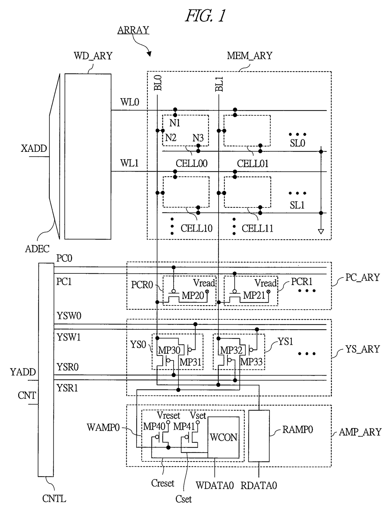
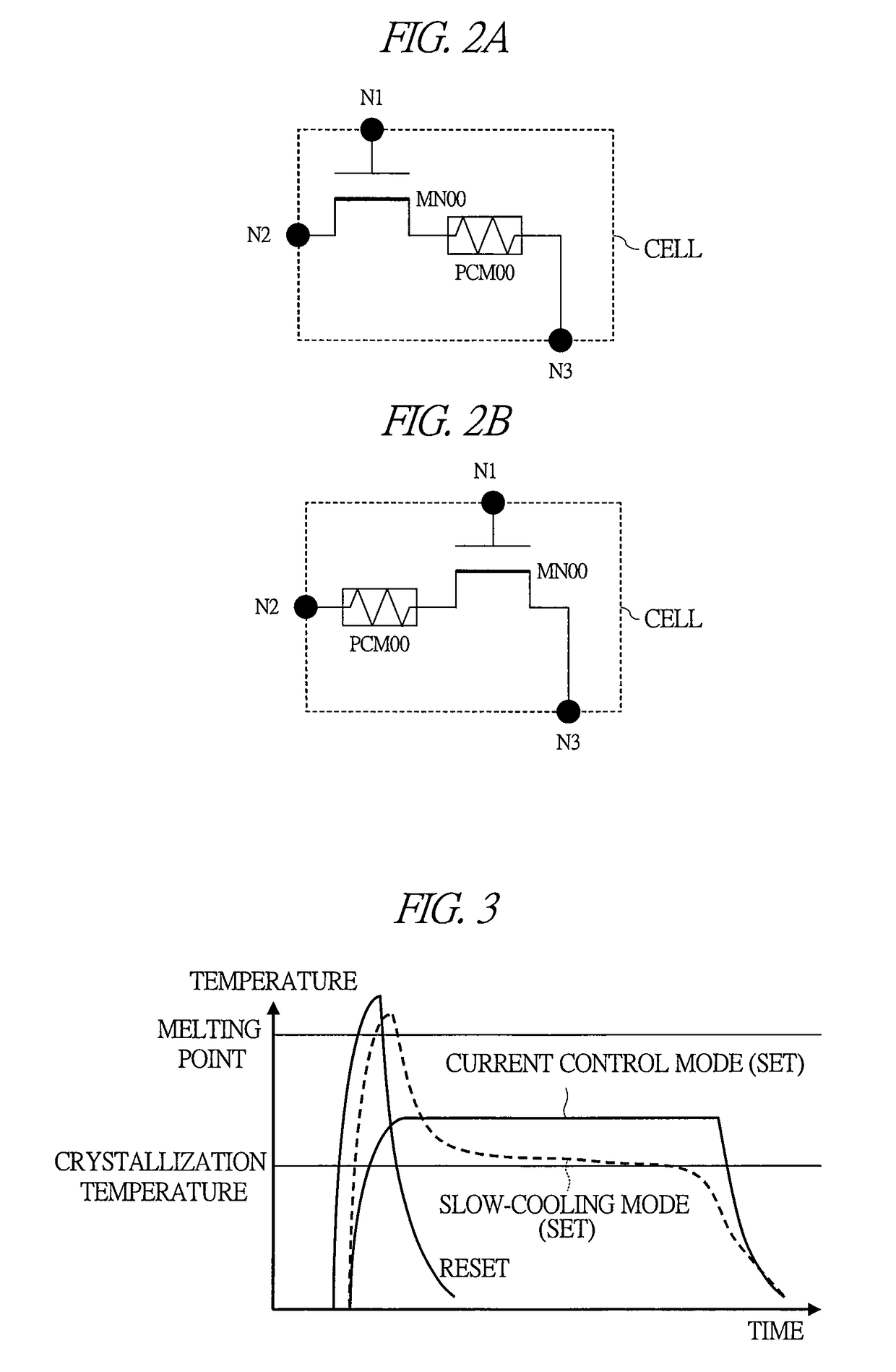
[0045]Hereinafter, several suitable cases of semiconductor device according to the present invention are described with reference to the drawings. Circuit elements forming each functional block of the embodiments are not particularly limited, and formed on a single semiconductor substrate such as that of single-crystal silicon through an integrated circuit technology for the known CMOS (complementary MOS transistor) and the like. Also, in the drawings, the gate of a PMOS transistor is provided with a circle sign, thereby distinguishing the PMOS transistor from an NMOS transistor. Herein, in the drawings, although connection of a substrate potential of a MOS transistor is not particularly depicted, a method of connection thereof is not particularly limited as long as the MOS transistor can normally operate. Furthermore, unless otherwise noted, low level of a signal is represented as “L” or “0” and high level thereof is represented as “H” or “1”.

[0046]

[0047]FIG. 1 is a schematic view ...


PUM


Abstract

At the time of, for example, a set operation (SET) for making a phase-change element in a crystalline state, a pulse of a voltage Vreset required for melting the element is applied to the phase-change element, and subsequently a pulse of a voltage Vset that is lower than Vreset and is required for crystallizing the element is applied thereto. And, the magnitude of this voltage Vset is then changed depending on the ambient temperature so that the magnitude of the voltage Vset is small as the temperature becomes high (TH). In this manner, a margin of a write operation between the set operation and a reset operation (RESET) for making the element to be in amorphous state is improved.

Description

TECHNICAL FIELD[0001]The present invention relates to a semiconductor device, more particularly, it relates to a semiconductor device such as a system LSI (microcomputer and the like) having an on-chip memory and a single non-volatile memory.BACKGROUND ART[0002]In order to achieve a high-speed and highly-integrated non-volatile memory, a phase-change memory has been developed. The phase-change memory is disclosed in Non-Patent Document 1 (“2002 IEEE International Solid-State Circuits Conference, Digest of Technical Papers”, pp. 202 to 203), Patent Document 1 (U.S. Pat. No. 6,487,113), and Patent Document 2 (U.S. Patent Application Publication No. 2004 / 0151023).[0003]For example, as disclosed in the Non-Patent Document 1, the phase-change memory stores information by using the fact that a phase-change element called a chalcogenide material has a resistance that differs according to its state. Rewriting of the phase-change element is performed by feeding current through the phase-chan...

Claims


Application Information

Patent Timeline
Patent Type & Authority Patents(United States)
IPC IPC(8): G11C11/00
CPCG11C13/0004G11C13/004G11C13/0069G11C7/04G11C2013/0054G11C2013/0092G11C2213/79
Inventor OSADA, KENICHIKITAI, NAOKIKAWAHARA, TAKAYUKIYANAGISAWA, KAZUMASA
Owner RENESAS ELECTRONICS CORP
Why Eureka
Try Eureka