Ferroelectric capacitor having three-dimensional structure, nonvolatile memory device having the same and method of fabricating the same

a three-dimensional structure and ferroelectric technology, applied in the direction of semiconductor devices, semiconductor/solid-state device details, electrical apparatus, etc., can solve the problems that the pzt layer may not have normal polarization characteristics and may not be beneficial as a ferroelectric, and achieve the effect of reducing the mutual diffusion of pb and si

Inactive Publication Date: 2011-03-22
SAMSUNG ELECTRONICS CO LTD
View PDF11 Cites 7 Cited by
  • Summary
  • Abstract
  • Description
  • Claims
  • Application Information

AI Technical Summary

Benefits of technology

[0008]Example embodiments provide a ferroelectric capacitor capable of reducing mutual diffusion of Pb and Si. Other example embodiments provide a nonvolatile memory device having the ferroelectric capacitor and a method of fabricating the nonvolatile memory device.

Problems solved by technology

A problem with the fabrication of semiconductor devices may be a side-effect caused by a mutual diffusion of materials.
If the crystal structure is changed, the PZT layer may not have normal polarization characteristics and may not be beneficial as a ferroelectric.

Method used


Image

  • Ferroelectric capacitor having three-dimensional structure, nonvolatile memory device having the same and method of fabricating the same
  • Ferroelectric capacitor having three-dimensional structure, nonvolatile memory device having the same and method of fabricating the same
  • Ferroelectric capacitor having three-dimensional structure, nonvolatile memory device having the same and method of fabricating the same

Examples


Embodiment Construction

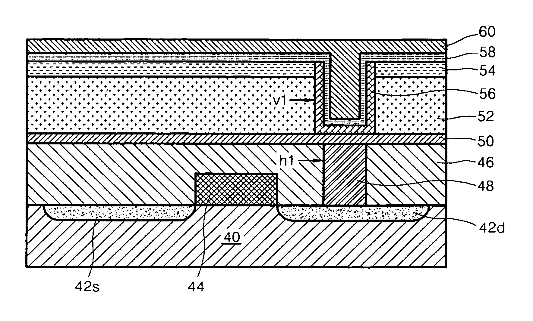
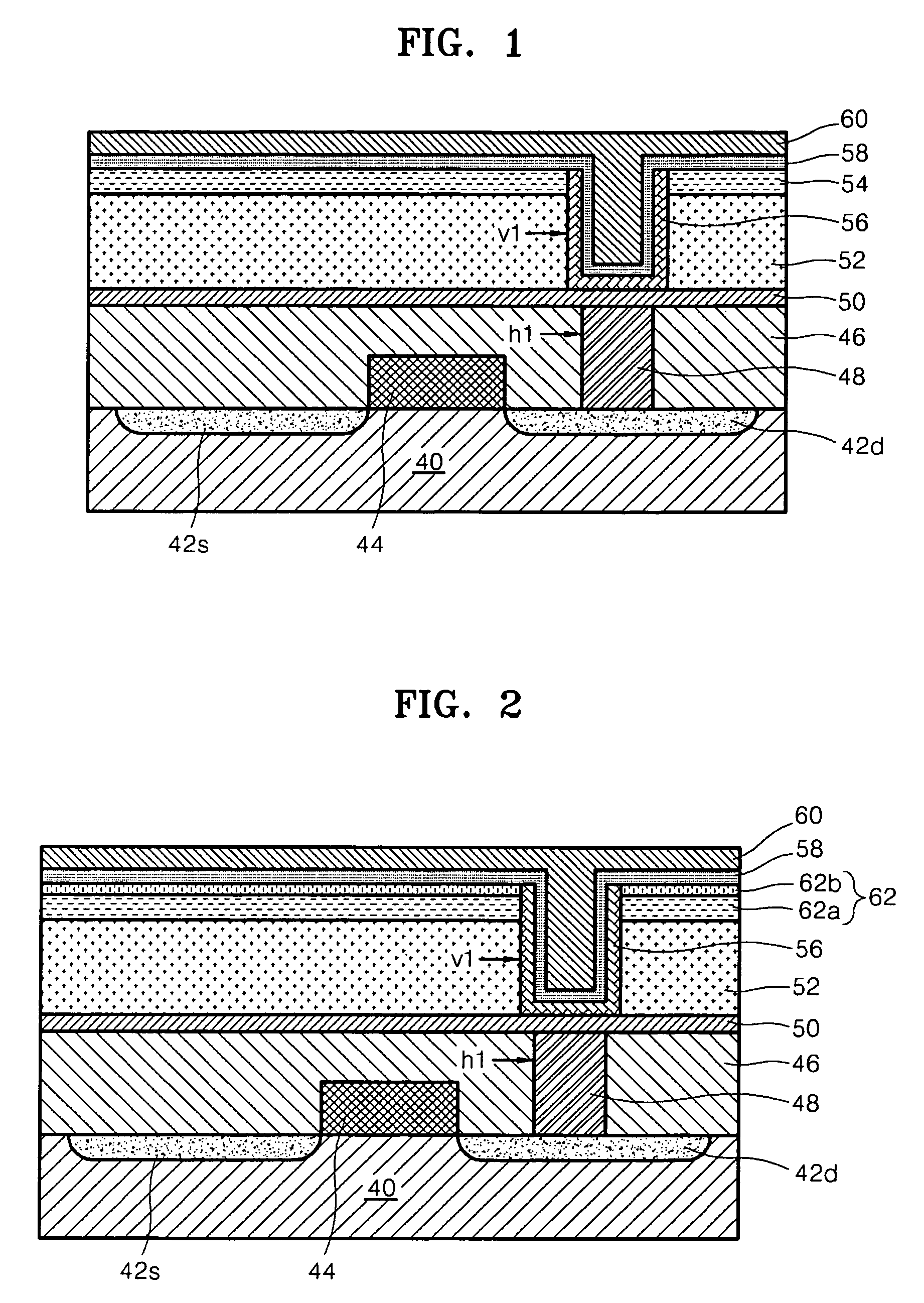
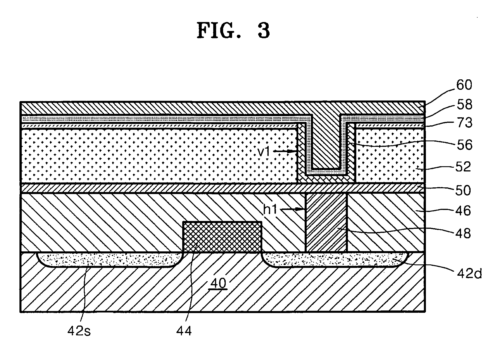
[0021]Example embodiments will now be described more fully hereinafter with reference to the accompanying drawings, in which example embodiments are shown. Example embodiments may, however, be embodied in many different forms and should not be construed as being limited to the embodiments set forth herein. Rather, these embodiments are provided so that this disclosure will be thorough and complete, and will fully convey the scope of example embodiments to those skilled in the art. In the drawings, the thicknesses of layers or regions are exaggerated for clarity.

[0022]Spatially relative terms, such as “beneath,”“below,”“lower,”“above,”“upper” and the like, may be used herein for ease of description to describe one element or feature's relationship to another element(s) or feature(s) as illustrated in the figures. It will be understood that the spatially relative terms are intended to encompass different orientations of the device in use or operation in addition to the orientation dep...


PUM

PropertyMeasurementUnit
ferroelectricaaaaaaaaaa
crystal structureaaaaaaaaaa
lengthaaaaaaaaaa

Abstract

A ferroelectric capacitor having a three-dimensional structure, a nonvolatile memory device having the same, and a method of fabricating the same are provided. The ferroelectric capacitor may include a trench-type lower electrode, at least one layer formed around the lower electrode, a ferroelectric layer (PZT layer) formed on the lower electrode and the at least one layer and an upper electrode formed on the ferroelectric layer. The at least one layer may be at least one insulating interlayer and the at least one layer may also be at least one diffusion barrier layer. The at least one layer may be formed of an insulating material excluding SiO2 or may have a perovskite crystal structure excluding Pb.

Description

PRIORITY STATEMENT[0001]This application claims priority under 35 U.S.C. §119 to Korean Patent Application No. 10-2005-0082439, filed on Sep. 5, 2005, in the Korean Intellectual Property Office (KIPO), the entire contents of which are incorporated herein by reference.BACKGROUND[0002]1. Field[0003]Example embodiments relate to a ferroelectric capacitor having a three-dimensional structure, a nonvolatile memory device having the same, and a method of fabricating the same.[0004]2. Description of the Related Art[0005]A problem with the fabrication of semiconductor devices may be a side-effect caused by a mutual diffusion of materials. The mutual diffusion of materials may result from the interface characteristics of component materials used in forming a semiconductor device and / or a higher processing temperature in the fabrication of semiconductor devices.[0006]Conventional semiconductor memory devices are being developed (e.g., a ferroelectric random access memory (FRAM) semiconductor ...

Claims


Application Information

Patent Timeline
Patent Type & Authority Patents(United States)
IPC IPC(8): H01L21/00H01L23/48H01L31/112
CPCH01L27/11502H01L27/11507H10B53/30H10B53/00H01L27/105
Inventor SHIN, SANG-MINPARK, YOUNG-SOOKOO, JUNE-MOBAE, BYOUNG-JAESONG, I-HUNKIM, SUK-PIL
Owner SAMSUNG ELECTRONICS CO LTD
Why Eureka
Try Eureka