Type-II superlattice structure based on indium arsenide and preparation method

A technology of superlattice and indium arsenide, applied in the direction of final product manufacturing, sustainable manufacturing/processing, electrical components, etc., can solve the problem of low superlattice growth temperature, achieve growth temperature increase, improve material performance, avoid The effect of frequent switching of As valve

Inactive Publication Date: 2016-07-20
SHANGHAI INST OF TECHNICAL PHYSICS - CHINESE ACAD OF SCI
View PDF0 Cites 2 Cited by
  • Summary
  • Abstract
  • Description
  • Claims
  • Application Information

AI Technical Summary

Problems solved by technology

[0005] 1. The problem of low superlattice growth temperature due to the existence of the InSb interface compensation layer;

Method used


Image

  • Type-II superlattice structure based on indium arsenide and preparation method
  • Type-II superlattice structure based on indium arsenide and preparation method

Examples


Embodiment 1

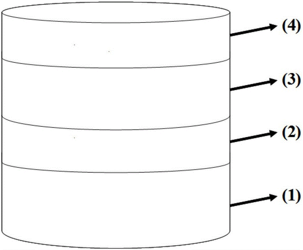
[0025] According to the content of the invention, we have prepared a type II superlattice material, and its specific structure is:

[0026] The thickness of the InAs layer 1 is 2.1 nm;

[0027] The thickness of the GaAs layer 2 is 0.0 nm;

[0028] GaAs x Sb 1-x The thickness of layer 3 is 2.1 nm, and the ratio x is 0.09;

[0029] The thickness of the GaAs layer 4 is 0.0 nm.

Embodiment 2

[0031] According to the content of the invention, we prepared a second type II superlattice material, and its specific structure is:

[0032] The thickness of the InAs layer 1 is 6.6 nm;

[0033] The thickness of the GaAs layer 2 is 0.1 nm;

[0034] GaAs x Sb 1-x The thickness of layer 3 is 2.7 nm, and the ratio x is 0.02;

[0035] The thickness of the GaAs layer 4 is 0.1 nm.

Embodiment 3

[0037] According to the content of the invention, we prepared a third type II superlattice material, and its specific structure is:

[0038] The thickness of the InAs layer 1 is 10.5 nm;

[0039] The thickness of the GaAs layer 2 is 0.15 nm;

[0040] GaAs x Sb 1-x The thickness of layer 3 is 3.6 nm, and the ratio x is 0.01;

[0041] The thickness of the GaAs layer 4 is 0.15 nm.


PUM

PropertyMeasurementUnit
thicknessaaaaaaaaaa
thicknessaaaaaaaaaa
thicknessaaaaaaaaaa

Abstract

The invention discloses a type-II superlattice structure based on indium arsenide and a preparation method. The type-II superlattice structure based on indium arsenide comprises an InAs layer, a GaAs layer, a GaAsxSb1-xlayer and a GaAs layer from bottom to top, and is characterized in that: (1) an original GaSb substrate is replaced with an InAs substrate, so that the growth temperature of superlattices is substantially increased, and the increasement of the growth temperature is conductive to increasing a diffusion length of surface atoms, thereby being more conductive to the two-dimensional growth of materials and the reduction of material defect density; (2) an As valve is always in an open state during the whole growth process of type-II superlattices, so that a GaAsSb ternary compound is formed due to the outflow of partial As when growing a GaSb layer, growth temperature of the layers tends to be uniform due to the existence of the common element As in the layers, and the counterdiffusion at interfaces is reduced; (3) variation of thickness of the InAs layer has small influence on mismatching of the InAs-based type-II superlattices, the growth difficulty of long waves materials, particularly extremely-long-wave materials, is extremely reduced, and the performance and quality of the materials can be more easily improved.

Description

technical field [0001] The invention relates to a type II superlattice material, in particular to a new type II superlattice structure based on an indium arsenide substrate and a preparation method, which are applied to medium-wave, long-wave and very long-wave infrared focal plane detectors. Background technique [0002] InAs / GaSb type II superlattice materials are the preferred materials for the third-generation infrared focal plane detectors. In recent years, the United States, Germany, Japan and other countries have been vigorously developing infrared detection technology based on this type II superlattice. The InAs / GaSb heteromaterial system has a very special energy band arrangement structure. The forbidden band width of InAs is smaller than the valence band offset of InAs / GaSb, so the bottom of the conduction band of InAs is below the top of the valence band of GaSb, forming a type II supercrystal. grid. This results in (1) electrons and holes are spatially separated...

Claims


Application Information

Patent Timeline
Patent Type & Authority Applications(China)
IPC IPC(8): H01L31/0352H01L31/18
CPCH01L31/0304H01L31/0352H01L31/035236H01L31/18H01L31/1844Y02P70/50
Inventor 王芳芳陈建新徐志成余成章
Owner SHANGHAI INST OF TECHNICAL PHYSICS - CHINESE ACAD OF SCI
Why Eureka
Try Eureka