Long-wavelength LED epitaxial wafer, chip and preparation method thereof

An LED chip, long-wavelength technology, used in electrical components, circuits, semiconductor devices, etc., can solve problems such as increased cost, increased manufacturing difficulty, environmental pollution, etc., to achieve the effect of improving brightness

Pending Publication Date: 2019-07-12
东莞市中晶半导体科技有限公司
View PDF0 Cites 0 Cited by
  • Summary
  • Abstract
  • Description
  • Claims
  • Application Information

AI Technical Summary

Problems solved by technology

However, the gallium nitride used in the prior art cannot directly emit red light. In order to emit white light, it is necessary to excite blue light or green light through a specific phosphor, so that it emits white light after excitation, so as to be used in the field of daily lighting. , but because phosphors are toxic and harmful, environmental pollution and other factors, they have received a lot of environmental protection attention in recent years, so major companies have begun to avoid the use of phosphors, and everyone is doing their best to study the use of healthy and safe alternatives
In fact, in addition to this, in order to obtain white light, it can also be prepared by mixing blue light, green light, and red light in theory. However, in the prior art, red light is mainly prepared from gallium arsenide. Performance, such as light decay period, service life, etc., especially the photoelectric performance can not be compared with the blue and green light prepared by gallium nitride, so in the process of white light preparation and daily lighting applications, everyone has given up using arsenide Gallium

Method used


Image

  • Long-wavelength LED epitaxial wafer, chip and preparation method thereof
  • Long-wavelength LED epitaxial wafer, chip and preparation method thereof
  • Long-wavelength LED epitaxial wafer, chip and preparation method thereof

Examples


Embodiment 1

[0052] Embodiment 1 0

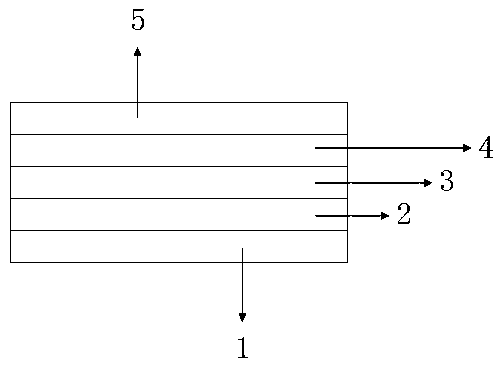
[0053] The long-wavelength LED epitaxial barrier wafer of the present invention such as Figure 4 As shown, including: sapphire substrate 1, buffer layer 2, n-type CaN3, quantum well 41, p-type CaN5, the prior art quantum well 4 has been improved, and the quantum well is AlxInyCa(1-x-y)N quantum well, x=0.1, y=0.4. The organic growth source containing C is introduced into the reaction chamber to participate in the growth of quantum wells under the catalysis of Cl2 or HCl. The growth temperature is controlled between 700°C and 990°C, and the temperature difference w between the well and epitaxy growth is controlled at about 80°C to control the quantum well growth. The well growth rate is about 0.6A / sec, the quantum wells are more than 7 pairs, and the concentration range of C in the quantum wells is 10 16 ——10 20 cm -3 , grow P-type CaN5 on the quantum well 41, and control the total thickness of the epitaxial barrier crystal layer wi...

Embodiment 2

[0055] The long-wavelength LED epitaxial barrier wafer of the present invention such as Figure 5 Shown, comprise: sapphire substrate 1, buffer layer 2, n-type CaN3, AlxInyCa (1-x-y) N quantum well comprises (quantum well 41, quantum well 42), p-type CaN5, carries out to prior art quantum well 4 Improvement is made to make quantum wells greater than or equal to 7 pairs. Quantum well 42 is the first, second and third pair of quantum wells wherein there is no deposition distribution of C. Quantum well 41 is the quantum well after the third pair of quantum wells, where x= 0.1, y=0.5, when the fourth pair of quantum wells grows, the trimethylaluminum source enters the reaction chamber to participate in the growth of quantum wells under the catalysis of Cl2 or HCl, and the growth temperature is controlled between 700°C and 990°C, where the wells and The epitaxy growth temperature difference w is controlled at about 70°C, and the growth rate is controlled at about 0.5A / sec, so that ...

Embodiment 3

[0057] like Figure 4 As shown, the long-wavelength LED epitaxial barrier wafer preparation method of the present invention comprises;

[0058] a Put the sapphire substrate 1 into the MOCVD reaction chamber;

[0059] b Epitaxial growth buffer layer 2 and n-type CaN3 on sapphire substrate 1;

[0060] c After growing n-type CaN3 in the epitaxial barrier crystal, start to grow AlxInyCa(1-x-y)N quantum well, where x=0.23, y=0.51. Control the epitaxial growth temperature at about 860°C, feed trimethylgallium as the gallium source in the reaction chamber, and feed chlorine gas as the catalyst at the same time, control the growth rate of the quantum well to about 0.6A / sec, and the growth temperature difference between the well and the epitaxial is about 55°C , the concentration range of C in the quantum well 41 is 10 17 cm -3 On the left and right, there are C-stacked multi-quantum wells 41 distributed in the growth of epitaxial barrier crystals, and the number of quantum wells 4...


PUM

PropertyMeasurementUnit
Thicknessaaaaaaaaaa

Abstract

The invention discloses a preparation method of a long-wavelength LED epitaxial wafer. The preparation step comprises a step of placing an epitaxial substrate into an epitaxial growth reaction chamber, and a step of growing a CaN epitaxial layer on the epitaxial substrate, growing a GaN buffer layer on the surface of the epitaxial substrate, growing an n-type Can on the GaN buffer layer, growing aquantum well on the n-type CaN, and growing a p-type CaN on the quantum well, wherein the thickness of the CaN epitaxial barrier is h, the thickness is controlled to be larger than or equal to 0.35 micrometers and smaller than or equal to 6 micrometer. The electrical performance of an LED prepared by a gallium-nitride-based long-wavelength LED epitaxial wafer prepared by the invention is consistent with the electrical performance of a blue-green CaN-based LED.

Description

technical field [0001] The invention relates to an LED epitaxial barrier wafer. More specifically, the present invention relates to a long-wavelength LED epitaxial barrier wafer, chip and preparation method thereof. Background technique [0002] In the prior art, gallium arsenide diodes emit red light, gallium phosphide diodes emit green light, silicon carbide diodes emit yellow light, and gallium nitride diodes emit blue light. Gallium nitride is a wide bandgap compound semiconductor material, which has the characteristics of blue light emission, high temperature, high frequency, high voltage, high power, acid resistance, alkali resistance, corrosion resistance, etc. It is the most important semiconductor after germanium, silicon and gallium arsenide As one of the materials, it occupies an important position in the field of blue light and ultraviolet optoelectronics technology, and it is also an ideal material for making high-temperature and high-power semiconductor devi...

Claims


Application Information

Patent Timeline
IPC IPC(8): H01L33/04H01L33/32H01L33/00
CPCH01L33/04H01L33/32H01L33/005
Inventor 颜建锋敖辉彭泽洋庄文荣孙明
Owner 东莞市中晶半导体科技有限公司
Why Eureka
Try Eureka