Method for preparing gallium-nitride-based photoelectric detector based on graphene insertion layer structure

A photodetector and gallium nitride-based technology, applied in the field of microelectronics, can solve problems such as increased dark current of devices, poor quality of nitride materials, and reduced quality of gallium nitride, so as to increase growth temperature, improve quality, and improve quality effect

Inactive Publication Date: 2018-11-23
XIDIAN UNIV
View PDF6 Cites 2 Cited by
  • Summary
  • Abstract
  • Description
  • Claims
  • Application Information

AI Technical Summary

Problems solved by technology

[0004] However, the shortcomings of this method are: first, since the method is epitaxial growth on a copper substrate, the growth temperature of the nitride material obtained in this way must be lower than the melting point of copper, and the higher quality nitride The growth temperature of aluminum should be higher than the melting point of copper, so the quality of the

Method used


Image

  • Method for preparing gallium-nitride-based photoelectric detector based on graphene insertion layer structure
  • Method for preparing gallium-nitride-based photoelectric detector based on graphene insertion layer structure

Examples


Embodiment 1

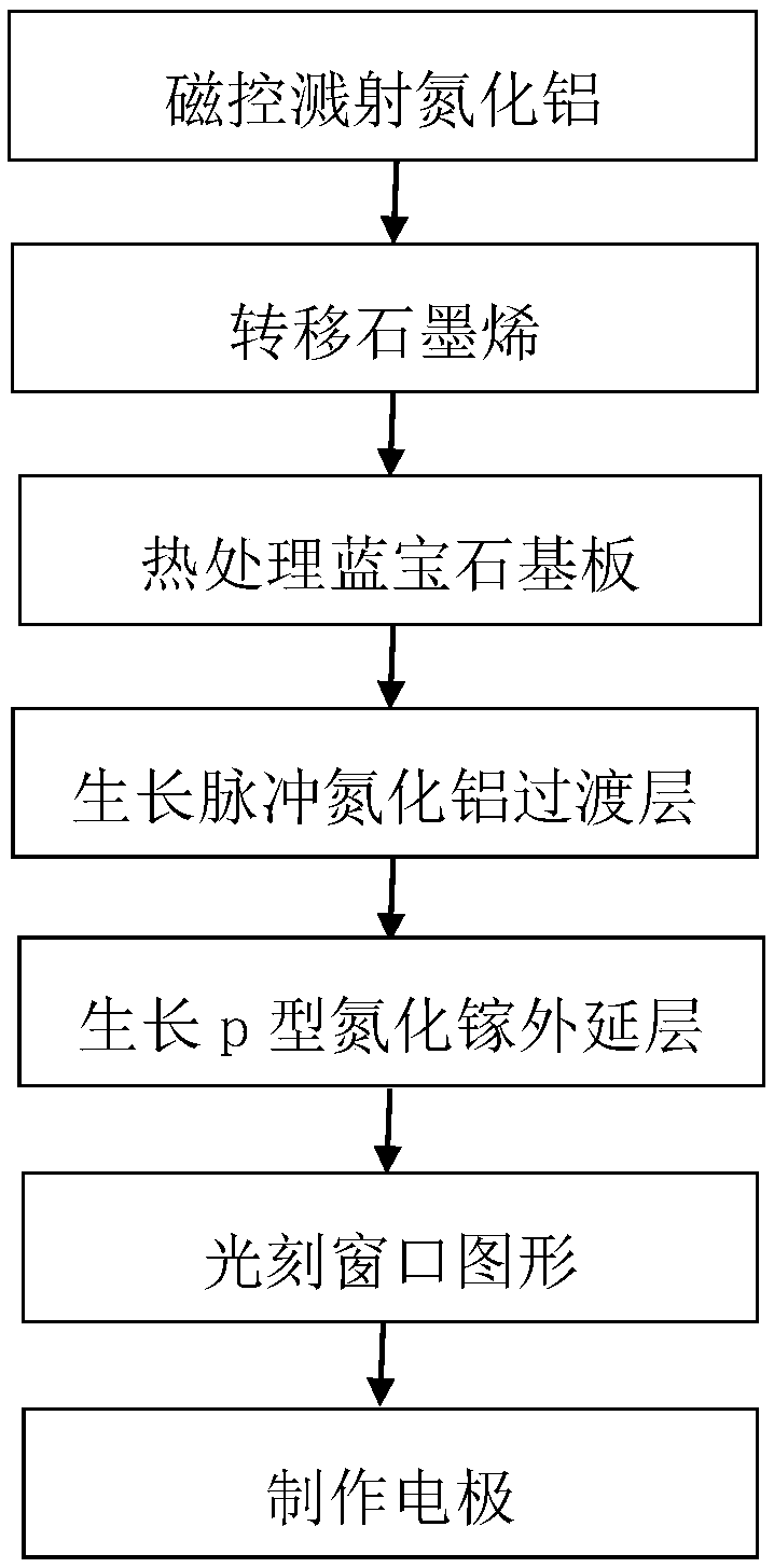
[0026] Example 1: Fabrication of a photodetector with a pulsed aluminum nitride transition layer thickness of 10 nm.

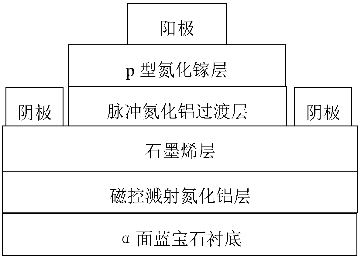
[0027] Step 1. Magnetron sputtering aluminum nitride film on α-plane sapphire substrate.

[0028] (1a) Place the α-face sapphire substrate in a magnetron sputtering system, the reaction chamber pressure is 1Pa, and nitrogen and argon are introduced into the system for 5 minutes;

[0029] (1b) Using aluminum with a purity of 99.999% as the target material, an aluminum nitride film with a thickness of 20nm is sputtered on the sapphire substrate by radio frequency magnetron sputtering to relieve the gap between the substrate and gallium nitride due to the crystal lattice Mismatch induced stress, resulting in sputtered AlN sapphire substrates.

[0030] Step 2. Transfer graphene onto magnetron sputtered aluminum nitride film.

[0031] (2a) adopt chemical vapor deposition method, grow the graphene layer of 0.34nm on copper substrate;

[0032] (2b) Place monolayer...

Embodiment 2

[0050] Example 2: Fabrication of a photodetector with a pulsed aluminum nitride transition layer thickness of 25 nm.

[0051] Step 1, magnetron sputtering aluminum nitride film on the α-plane sapphire substrate.

[0052] First place the α-plane sapphire substrate in the magnetron sputtering system, the pressure of the reaction chamber is 1Pa, and nitrogen and argon are introduced for 5 minutes, and then the aluminum with a purity of 99.999% is used as the target material, and the radio frequency magnetron sputtering is used. A 50nm aluminum nitride film was sputtered on the sapphire substrate to relieve the stress caused by lattice mismatch between the substrate and gallium nitride, and a sapphire substrate sputtered with aluminum nitride was obtained.

[0053] Step two, transfer the graphene onto the magnetron sputtered aluminum nitride film.

[0054] First adopt the chemical vapor deposition method to grow a 0.34nm graphene layer on the copper substrate; then place the sing...

Embodiment 3

[0065] Example 3: Fabrication of a photodetector with a pulsed aluminum nitride transition layer thickness of 50 nm.

[0066] Step A. Magnetron sputtering aluminum nitride thin film on α-plane sapphire substrate.

[0067] First, the α-face sapphire substrate was placed in a magnetron sputtering system, the reaction chamber pressure was 1 Pa, and nitrogen and argon were introduced for 5 minutes.

[0068] Then, using 99.999% pure aluminum as the target material, a 100nm thick AlN film was sputtered on the sapphire substrate by radio frequency magnetron sputtering to alleviate the lattice mismatch between the substrate and GaN. The resulting stress was obtained by sputtering AlN on a sapphire substrate.

[0069] Step B. Transfer graphene onto magnetron sputtered aluminum nitride film.

[0070] First, a graphene layer with a thickness of 0.34 nm is grown on a copper substrate by chemical vapor deposition;

[0071] Then, place the monolayer graphene in 64g / L (NH 4 ) 2 S 2 o ...


PUM

PropertyMeasurementUnit
Thicknessaaaaaaaaaa
Thicknessaaaaaaaaaa
Thicknessaaaaaaaaaa

Abstract

The invention discloses a method for preparing a gallium-nitride-based photoelectric detector based on a graphene insertion layer. The method is mainly used for solving the problems that in the priorart, a nitride material epitaxially grown on a copper substrate is poor in quality and is not provided with a transition layer. The method comprises the preparation steps that a magnetron sputtering aluminum nitride thin film is arranged on an alpha-surface sapphire substrate; graphene is transferred to the magnetron sputtering aluminum nitride thin film, and a sapphire substrate covered with thegraphene is obtained and heated; a pulsed aluminum nitride transition layer is grown on the heated sapphire substrate; a low-temperature gallium nitride layer is grown on the transition layer to obtain a gallium nitride substrate; and a window graph is photoetched on the gallium nitride substrate, and an electrode is manufactured. Magnetron sputtering aluminum nitride and the pulsed aluminum nitride transition layer are adopted, the graphene serves as the insertion layer, thus gallium nitride can grow on the substrate with the large lattice mismatch constant, the quality of the gallium-nitride-based photoelectric detector is improved, and the method can be used for manufacturing gallium-nitride-based photoelectric devices.

Description

technical field [0001] The invention belongs to the technical field of microelectronics, and in particular relates to a preparation method of a gallium nitride-based photodetector based on a graphene intercalation layer structure, which can be used in the preparation of gallium nitride-based photoelectric devices. Background technique [0002] Graphene is an emerging two-dimensional carbon nanomaterial, which has a zero band gap and thus has a high electron mobility, which can reach 15,000 cm at room temperature. 2 ·V -1 ·s -1 , it is the material with the lowest resistivity known so far. At the same time, it also has good light transmittance, and the light transmittance of a single layer is about 97.7%. Because of these characteristics, graphene has a good application prospect in the field of optoelectronic devices. At present, the third-generation wide-bandgap semiconductor materials represented by gallium nitride have been widely used in the fields of optoelectronic de...

Claims


Application Information

Patent Timeline
IPC IPC(8): H01L31/18H01L31/109
CPCH01L31/109H01L31/1852H01L31/1856Y02P70/50
Inventor 宁静沈雪王东张进成张弛陈智斌马佩军郝跃
Owner XIDIAN UNIV
Why Eureka
Try Eureka