Supercharge Your Innovation With Domain-Expert AI Agents!

Method for doping polysilicon and method for fabricating a dual poly gate using the same

a polysilicon and polysilicon technology, applied in the direction of semiconductor devices, basic electric elements, electrical equipment, etc., can solve the problems of limit of mass production, and deterioration of electrical characteristics of devices, so as to prevent dopant loss

Inactive Publication Date: 2011-04-05
SK HYNIX INC
View PDF11 Cites 3 Cited by
  • Summary
  • Abstract
  • Description
  • Claims
  • Application Information

AI Technical Summary

Benefits of technology

The present invention provides methods for doping polysilicon to prevent dopant loss during plasma doping and to increase the uniformity of doping concentration according to the depth of a layer inside. These methods involve forming layers of silicon over a substrate, doping them with impurities, and activating them. The invention also provides a method for fabricating a dual poly gate by forming a gate insulation layer, doping the silicon layers in the NMOS region and PMOS region, activating the dopants, and etching the silicon layers to form a gate pattern.

Problems solved by technology

However, if high-doping of a high concentration is applied using a typical beam-line implant, there may be limitations in mass production.
Therefore, an impurity concentration on the interface between the polysilicon and a gate oxide layer is low and, according thereto, electrical characteristics of a device become deteriorated.
Accordingly, electrical characteristics of a device become deteriorated.

Method used


Image

  • Method for doping polysilicon and method for fabricating a dual poly gate using the same
  • Method for doping polysilicon and method for fabricating a dual poly gate using the same
  • Method for doping polysilicon and method for fabricating a dual poly gate using the same

Examples


Embodiment Construction

[0021]Hereinafter, a method for doping polysilicon and a method for fabricating a dual poly gate using the same in accordance with the present invention will be described in detail with reference to the accompanying drawings.

[0022]It will be understood that when an element such as a layer, a film, a pattern and a region is referred to as being ‘on / under’ another element herein, it may be directly on / under the other element, and one or more intervening elements may also be present.

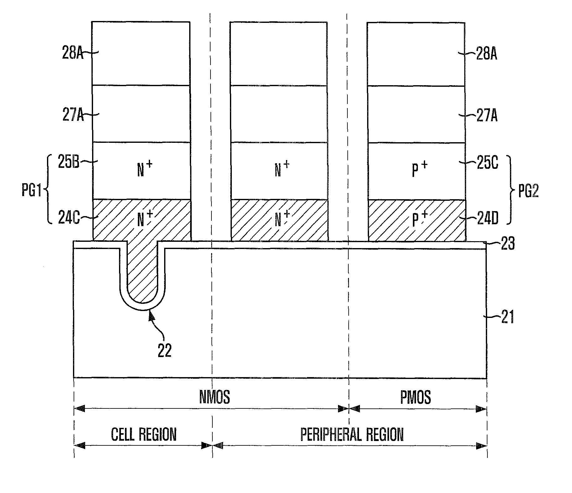
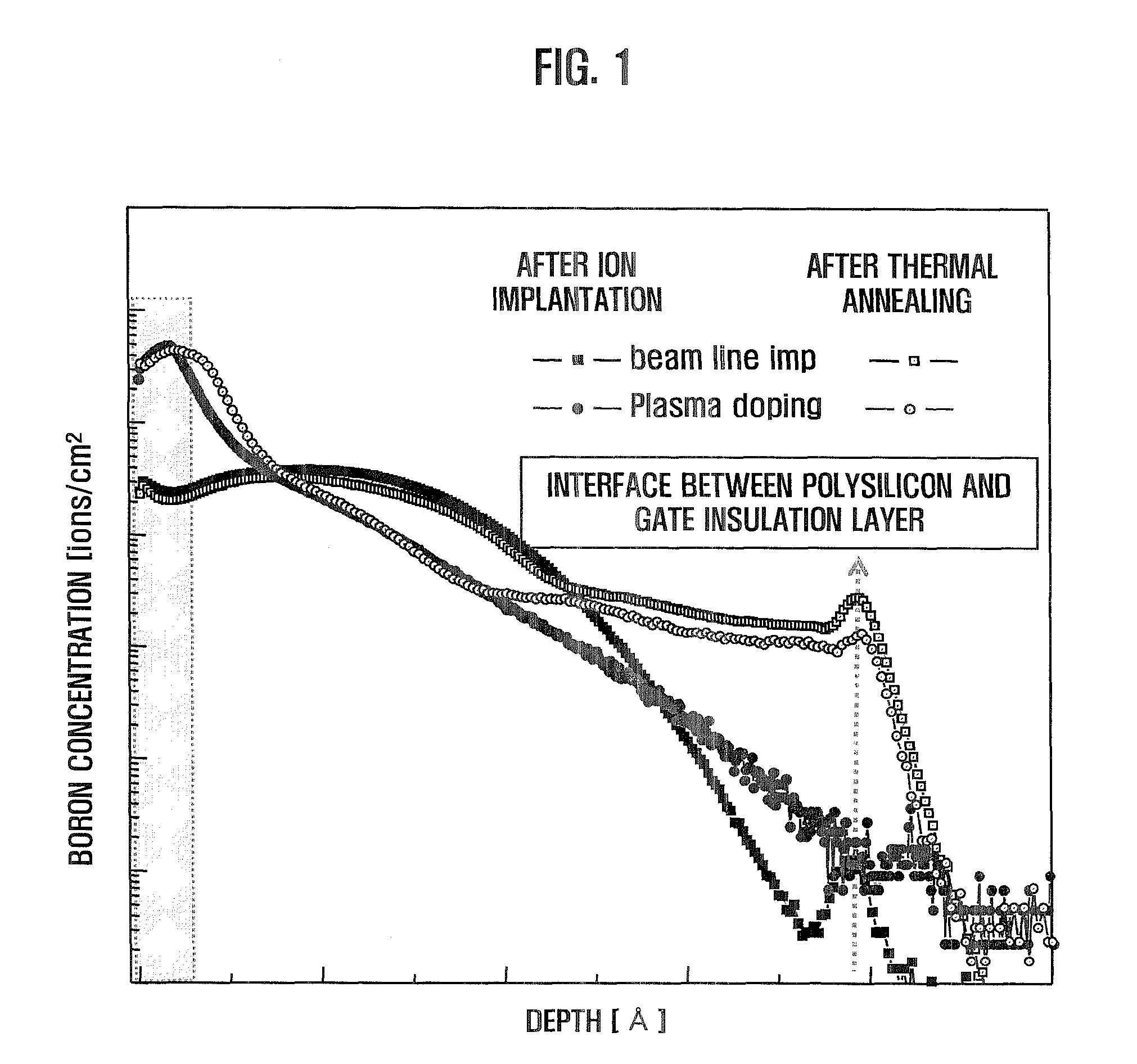
[0023]According to the present invention, a method for improving a doping profile during plasma doping includes forming a silicon layer using two separate operations. After forming a first silicon layer, thermal annealing is performed to crystallize the first silicon layer, such that the uniformity of a doping concentration according to the depth of a layer inside is improved during plasma doping. Additionally, a doping concentration at the interface between a polysilicon layer and a gate oxide layer is inc...


PUM

PropertyMeasurementUnit
temperatureaaaaaaaaaa

Abstract

A method for doping polysilicon improves a doping profile during plasma doping and includes forming a silicon layer using two separate operations. After forming a first silicon layer, thermal annealing is performed to crystallize the first silicon layer, such that the uniformity of a doping concentration according to the depth of a layer inside is improved during plasma doping. Additionally, a doping concentration at the interface between a polysilicon layer and a gate oxide layer is increased. A by-product deposition layer is reduced, which is formed on the surface of a polysilicon layer due to the increase of a doping concentration in a polysilicon layer. As a result, the dopant loss, which is caused by the removing and cleansing of an ion implantation barrier used during doping, is reduced.

Description

CROSS-REFERENCE TO RELATED APPLICATIONS[0001]The present invention claims priority of Korean patent application numbers 2007-0087658 and 2008-0036657, filed on Aug. 30, 2007, and Apr. 21, 2008, respectively, which are incorporated by reference in their entirety.BACKGROUND OF THE INVENTION[0002]The present invention relates to a semiconductor fabricating technique, and more particularly, to a method for doping polysilicon and a method for fabricating a dual poly gate using the same.[0003]It is well known that dual poly gates operate in a peripheral circuit of a dynamic random access memory (DRAM). Each dual poly gate includes an N-type polysilicon as a gate of an NMOS transistor and a P-type polysilicon as a gate of a PMOS transistor. If a gate of a PMOS transistor is formed of a P-type polysilicon unlike a typical structure where all the gates of NMOS and PMOS transistors are formed of an N-type polysilicon, a short channel effect is reduced, and also a drain saturation current Idsa...

Claims


Application Information

Patent Timeline
Patent Type & Authority Patents(United States)
IPC IPC(8): H01L21/336H01L21/00H01L21/20
CPCH01L21/02532H01L21/02667H01L27/10894H01L27/10876H01L21/02675H10B12/053H10B12/09
Inventor LEE, JIN-KUOH, JAE-GEUNHWANG, SUN-HWAN
Owner SK HYNIX INC
Features
  • R&D
  • Intellectual Property
  • Life Sciences
  • Materials
  • Tech Scout
  • Unparalleled Data Quality
  • Higher Quality Content
  • 60% Fewer Hallucinations
Learn More