
Power receiving device and power transfer system

a power receiving device and power transfer technology, applied in the direction of near-field systems using receivers, instruments, inductances, etc., to achieve the effect of increasing the efficiency of wireless electric power transfer

Active Publication Date: 2011-04-05
SONY CORP
View PDF8 Cites 181 Cited by
  • Summary
  • Abstract
  • Description
  • Claims
  • Application Information

AI Technical Summary

Benefits of technology

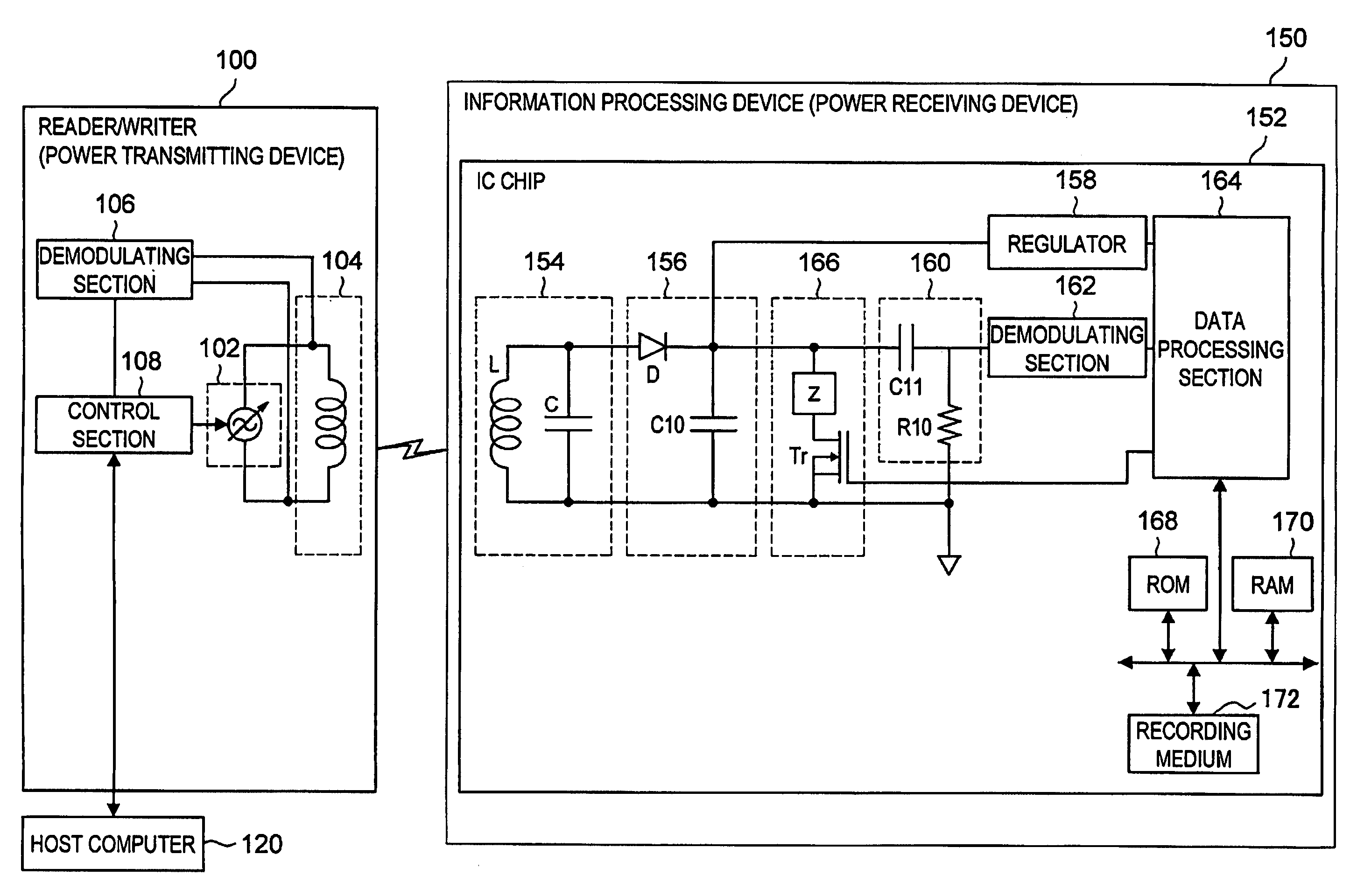
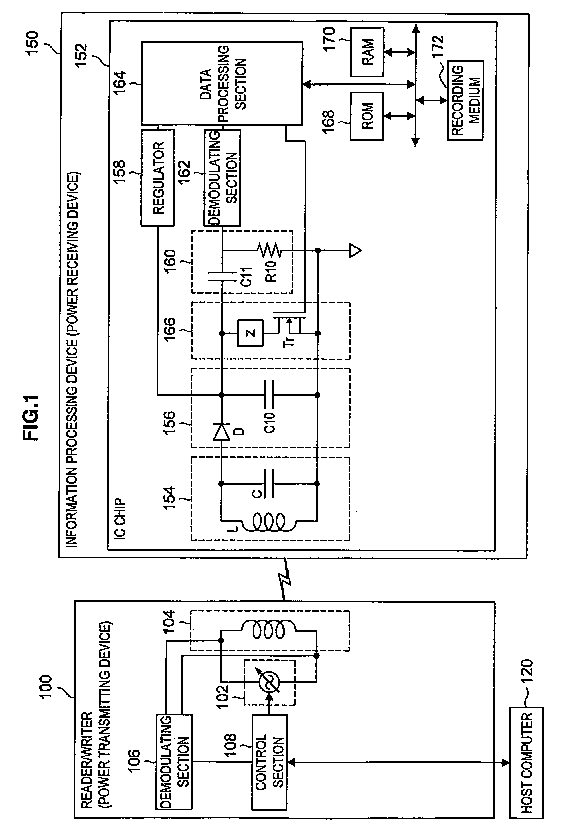
The patent text describes a power receiving device that can receive a carrier wave transmitted from a power transmitting device without contact and obtain electric power from it. The device includes a carrier receiving section, a processing section, and an impedance converting section. The carrier receiving section includes a communication antenna that has predetermined inductance and does not have an intermediate tap. The impedance converting section converts the impedance between the carrier receiving section and the processing section. This configuration allows for increased efficiency of wireless transfer of electric power without placing an intermediate tap in the communication antenna. The power transfer system also includes a power transmitting device that generates a carrier wave and a power receiving device that receives it. This further increases the efficiency of wireless transfer of electric power.

Problems solved by technology

However, because the size of a coil or a loop antenna is generally larger than the size of a resonance capacitor, leads of an intermediate tap or placement of a coupling coil may constitute a restriction on packaging.

Method used


Image

  • Power receiving device and power transfer system
  • Power receiving device and power transfer system
  • Power receiving device and power transfer system

Examples


third embodiment

[0130]The power receiving device 250 of the first embodiment described above has the configuration that the impedance converting circuit performs capacitive division to thereby perform impedance conversion, and the power receiving device 350 of the second embodiment has the configuration that the impedance converting circuit performs impedance conversion using the transformer. A method of impedance conversion according to embodiments of the present invention, however, is not limited to the use of capacitive division or the transformer. A power receiving device according to a third embodiment, which performs a different method of impedance conversion from the power receiving devices according to the first and second embodiments, is described hereinafter.

first configuration example

Configuration Example of the Power Receiving Device 550

[0131]FIG. 12 is an explanatory view showing an equivalent circuit of a first configuration example of a power receiving device according to a third embodiment of the present invention. FIG. 12 also shows the power transmitting device 200 which transmits a carrier wave.

[0132]A power receiving device 550 includes a carrier receiving circuit 552, an impedance converting circuit 554 and a processing circuit 556, like the power receiving device 250 of the first embodiment. Referring to FIG. 12, the carrier receiving circuit 552, the impedance converting circuit 554 and the processing circuit 556 respectively have the following configurations.

[0133](Carrier Receiving Circuit 552)

[0134]The carrier receiving circuit 552 is formed by a resonance circuit that is composed of an inductor L (communication antenna) having predetermined inductance which is not equipped with an intermediate tap and a capacitor having predetermined capacitance....

second configuration example

Configuration Example of the Power Receiving Device 650

[0142]Although the first configuration example of the power receiving device according to the third embodiment shown in FIG. 12 shows the case where the impedance converting circuit is formed by an inductor, the power receiving device according to the third embodiment is not limited thereto. FIG. 13 is an explanatory view showing an equivalent circuit of a second configuration example of the power receiving device according to the third embodiment of the present invention. FIG. 13 also shows the power transmitting device 200 which transmits a carrier wave.

[0143]A power receiving device 650 includes a carrier receiving circuit 652, an impedance converting circuit 654 and a processing circuit 656, like the power receiving device 550 of the first configuration example. Referring to FIG. 13, the carrier receiving circuit 652, the impedance converting circuit 654 and the processing circuit 656 respectively have the following configur...


PUM

PropertyMeasurementUnit
frequencyaaaaaaaaaa
electric poweraaaaaaaaaa
inductanceaaaaaaaaaa

Abstract

There is provided a power receiving device capable of receiving a carrier wave transmitted from a power transmitting device without contact and obtaining electric power from the received carrier wave, which includes a carrier receiving section at least including a communication antenna having predetermined inductance and not equipped with an intermediate tap, to receive the carrier wave and generate an induced voltage corresponding to the carrier wave, a processing section to generate a drive voltage based on the induced voltage and perform data processing using the generated drive voltage, and an impedance converting section to convert impedance between the carrier receiving section and the processing section.

Description

CROSS REFERENCES TO RELATED APPLICATIONS[0001]The present invention contains subject matter related to Japanese Patent Application JP 2007-226572 filed in the Japan Patent Office on Aug. 31, 2007, the entire contents of which being incorporated herein by reference.BACKGROUND OF THE INVENTION[0002]1. Field of the Invention[0003]The present invention relates to a power receiving device and a power transfer system.[0004]2. Description of the Related Art[0005]Information processing devices capable of communicating without contact with a reader / writer (or an information processing device having a reader / writer function), such as a non-contact integrated circuit (IC) card, a radio frequency identification (RFID) tag and a cellular phone equipped with a non-contact IC chip, have come into widespread use.[0006]A reader / writer and an information processing device such as an IC card or a cellular phone communicate with each other by using a magnetic field at a specific frequency such as 13.56...

Claims


Application Information

Patent Timeline
Patent Type & Authority Patents(United States)
IPC IPC(8): H01F27/42G06K19/07H04B5/48
CPCG06K19/0701H02J17/00G06K19/0723H02J50/12H02J50/80
Inventor TANAKA, KATSUYUKI
Owner SONY CORP
Learn More