Electronic package having stress buffer layer on mounting surface thereof, and method for manufacturing same

a technology of stress buffer layer and mounting surface, which is applied in the direction of basic electric elements, generators/motors, solid-state devices, etc., can solve the problems of high cost of ceramic package, surface mount devices may be subjected to stress and damage, and glass has less strength than cerami

Inactive Publication Date: 2011-04-12
SEIKO INSTR INC
View PDF12 Cites 16 Cited by
  • Summary
  • Abstract
  • Description
  • Claims
  • Application Information

AI Technical Summary

Benefits of technology

[0016]In view of the above, it is an object of the present invention to provide an electronic component, and the like, that can withstand stress from a printed circuit board, and the like, after being mounted.
[0027]In accordance with the present invention, the stress buffer member disposed between external electrodes and a package allows an electronic component to withstand stress from a printed circuit board, or the like, after the electronic component is mounted.

Problems solved by technology

However, the cost for the package made of ceramic is high.
However, glass has less strength than ceramic, and the surface mount devices are directly mounted on the printed circuit board.
So, when the printed circuit board bends after mounting the surface mount devices, the surface mount devices may be subjected to stress and damaged (for example, the glass may become cracked).
However, the chemical processing may indeed strengthen the glass, but it causes a problem of reducing the strength due to the history of the heat treatment.
The reason of this problem may be that the potassium ion near the glass surface diffuses into or within the glass.
Also, other problems are that the glass case may become warped, that cutting may become difficult after wafer processing, and that a cutting surface is not strengthened after cutting the glass.

Method used


Image

  • Electronic package having stress buffer layer on mounting surface thereof, and method for manufacturing same
  • Electronic package having stress buffer layer on mounting surface thereof, and method for manufacturing same
  • Electronic package having stress buffer layer on mounting surface thereof, and method for manufacturing same

Examples


first embodiment

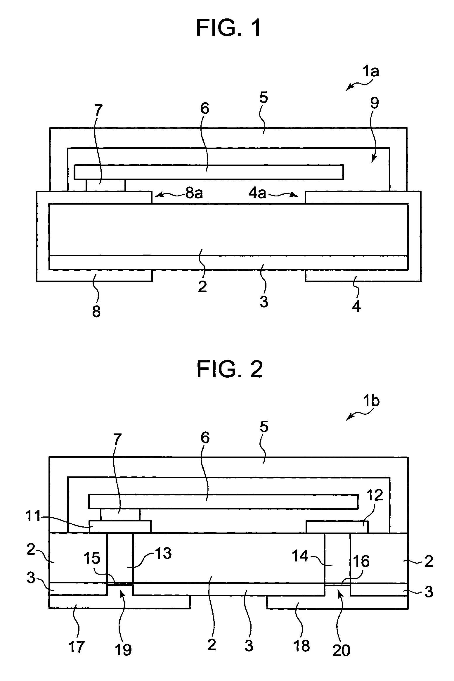
[0043]FIG. 1 is a diagram showing the cross-section of an electronic component 1a in accordance with an embodiment of the invention.

[0044]The electronic component 1a includes a base 2, a stress buffer layer 3, an external electrode 4, an external electrode 8, a crystal resonator 6, a supporting member 7, and a lid 5.

[0045]Note that, when being mounted, the bottom surface of the external electrode 4 (the side facing the stress buffer layer 3) is soldered to the printed circuit board, and FIG. 1 is the cross-sectional view of the electronic component 1a viewed in parallel to the surface of the printed circuit board.

[0046]So, in the following, the side of the electronic component 1a facing the printed circuit board is referred to as “bottom surface side” when being mounted, and the side opposite to the bottom surface side is referred to as “top surface side.”

[0047]The crystal resonator 6 includes, for example, a tuning fork type crystal resonator, and the proximal end of the tuning for...

second embodiment

[0078]FIG. 2 is a cross-sectional view of an electronic component 1b in accordance with a second embodiment.

[0079]In FIG. 2, components like those in the electronic component 1a are denoted by like numerals, and the description is simplified or omitted.

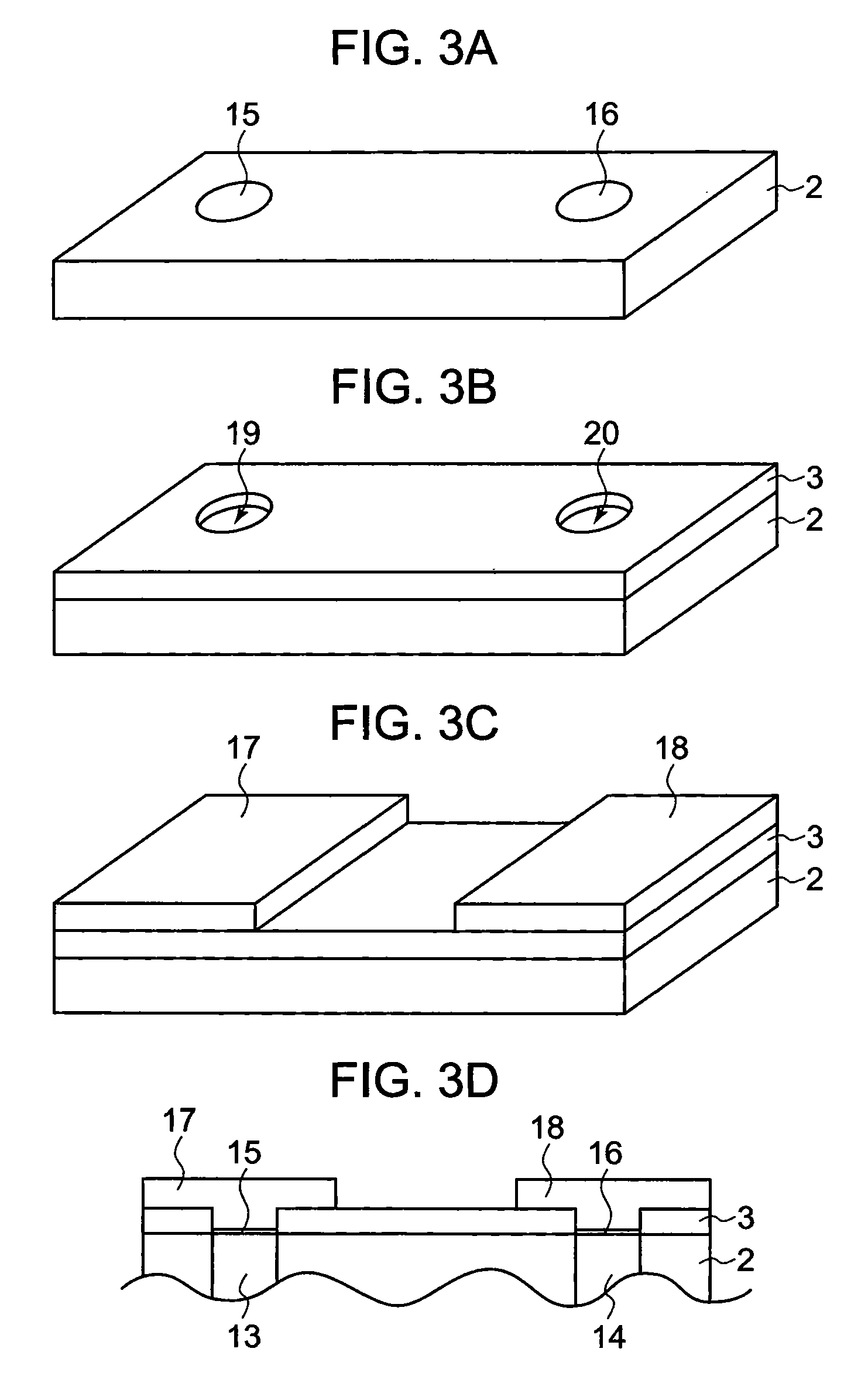
[0080]In the electronic component 1b, two through-holes are formed in a base 2, within which through-electrodes 13, 14 are formed, respectively.

[0081]For example, the through-electrodes 13, 14 are formed by heat-treating and curing conductive paste such as glass silver paste, or made of metal bar, metal plating, or the like. The edge surfaces of the through-electrodes 13, 14 on the top surface side of the base 2 are connected to internal wirings 11, 12 disposed on two electrodes of a crystal resonator 6, respectively.

[0082]On the edge surfaces of the through-electrodes 13, 14 on the bottom surface side, conductive connecting layers 15, 16 are provided to enhance adhesion between external electrodes 17, 18 and the through-electrodes 13...

third embodiment

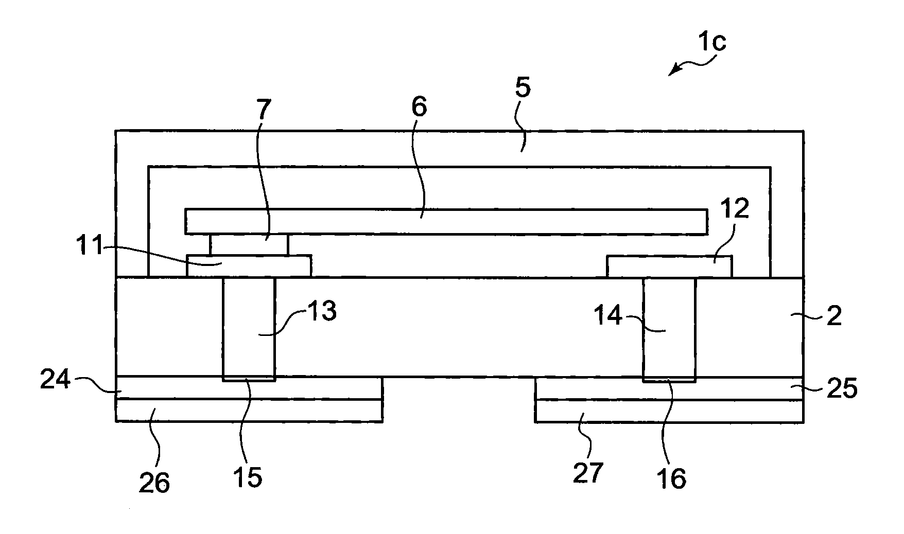
[0103]FIG. 4 is a cross-sectional view of an electronic component 1c in accordance with a third embodiment.

[0104]In FIG. 4, components like those in the electronic component 1b are denoted by like numerals, and the description is simplified or omitted.

[0105]In the electronic component 1c, stress buffer layers 24, 25 that are conductive are formed at the locations of through-electrodes 13, 14 on the bottom surface of a base 2. The stress buffer layers 24, 25 are electrically connected to the through-electrodes 13, 14 via connecting layers 15, 16, respectively.

[0106]As for the material of the stress buffer layer 24, 25, for example, the resin used for the stress buffer layer 3 of the electronic component 1a mixed with a conductive filler can be used, the conductive filler being the mixture of one or more types of single metals or alloys of Ag, Au, Cu, Ni, Sn, or the like.

[0107]On the bottom surfaces of the stress buffer layers 24, 25, external electrodes 26, 27 are formed, respectivel...


PUM


Abstract

An electronic component capable of withstanding stress from a printed circuit board or the like is provided. In an electronic component, a cavity hermetically sealed by a base and a lid is formed. In the cavity, a crystal resonator is supported by a supporting member over the top surface of the base. The base is made of glass. A stress buffer layer made of a conductive resin or the like is formed over the whole bottom surface of the base. An external electrode and an external electrode that are in continuity with the electrodes of the crystal resonator individually extend to the bottom surface of the stress buffer layer via the side surfaces of the base and stress buffer layer. The thus configured electronic component is surface-mounted by, for example, soldering the external electrode and external electrode formed on the bottom surface of the stress buffer layer to a printed circuit board.

Description

RELATED APPLICATIONS[0001]This application is a continuation of PCT / JP2009 / 052184 filed on Feb. 9, 2009, which claims priority to Japanese Application No. 2008-032046 filed on Feb. 13, 2008. The entire contents of these applications are incorporated herein by reference.BACKGROUND OF THE INVENTION[0002]1. Field of the Invention[0003]The present invention relates to an electronic component, an electronic apparatus, and a base member manufacturing method, and for example, relates to an electronic component with a crystal resonator housed in a glass package.[0004]2. Description of the Related Art[0005]In recent years, surface mount devices with an electronic device such as a crystal resonator and semiconductor housed in a package are widely used.[0006]Each surface mount device has external electrodes on the bottom surface, or the like, and is mounted by soldering the external electrodes onto the surface of a printed circuit board.[0007]One example of the package is a ceramic base to whi...

Claims


Application Information

Patent Timeline
Patent Type & Authority Patents(United States)
IPC IPC(8): H01L41/08
CPCH01L23/562H01L41/053H03H9/1021H01L2924/09701H03H9/02133H03H9/0552H01L2924/0002H01L2924/00H10N30/88
Inventor TAKEUCHI, HITOSHISATO, KEIJIARATAKE, KIYOSHINUMATA, MASASHI
Owner SEIKO INSTR INC
Why Eureka
Try Eureka