Methods and apparati for making thin semi-conductor wafers with locally controlled regions that are relatively thicker than other regions and such wafers

a technology of semi-conductor wafers and local control, applied in the direction of sustainable manufacturing/processing, polycrystalline material growth, final product manufacturing, etc., can solve the problems of reducing the electronic affecting the quality causing the loss of thin semiconductor wafers, etc., to achieve less risk of damage, less cost, and less cost

Active Publication Date: 2017-02-23
CUBICPV INC
View PDF6 Cites 11 Cited by
  • Summary
  • Abstract
  • Description
  • Claims
  • Application Information

AI Technical Summary

Benefits of technology

[0029]In another embodiment, specifically chosen regions within the interior of the wafer can be relatively thicker than other regions. For example, a wafer can be made having stripes of greater thickness in the regions which will later receive the interconnection bus bars. FIG. 2 shows an example of a wafer with such thickened stripes. Such stripes provide sturdier, more crack resistant regions to withstand the stresses of electrical connections, such as soldering, or adhesives to thicker metal conductors.
[0031]Another invention hereof is a solar cell made using such thick bordered, or thick regions, thin interior wafers. They are lighter, less expensive, more durable and more efficient than solar cells having conventional, uniform thickness semiconductor wafers as their solar energy collectors. The electrical connections required to connect one cell to another to fabricate a module can be provided to the wafers with less risk of damage.
[0037]Considering, for example, to form a wafer having a relatively thicker perimeter region, this can be achieved by controlling the heat flow from the semi-conductor melt to the template, such that there is more heat extracted from the molten material around the perimeter, in the regions where it is desired that the wafer be thicker, as compared to the interior region. The wafer as formed will be thicker around the perimeter than it is in the interior. Similarly, for relatively thicker stripes or other geometries, particularly to be associated with electrical connections, relatively more heat extracted at the locations desired to be relatively thicker, will result in such relatively greater thickness, as compared to the regions where there is relatively less heat extracted.

Problems solved by technology

Generally, greater increases are associated with lower wafer electronic quality.
However, such thinner wafers have been found to break during cell fabrication, electrical interconnection and encapsulation into a module.
For typical cell structures including PERC using multi-crystalline silicon material, making wafers thinner than 80 microns does not provide any further appreciable efficiency gain.
During cell fabrication, wafers often break by propagation of a defect from an edge of the wafer.
Edge defects include cracks and thin spots.
Further, during handling, new cracks and defects are created at the edges, because they are the locations of contact with other pieces of equipment during the manufacturing process.
Cracks starting from an edge are a problem during cell making and module fabrication.
In general, it has been found that with presently used machinery and methods, PV wafers that are thinner than 150 microns are damaged with unacceptable frequency to be practical.
Further, if improperly bent, the wire can actually touch the edge of the cell, thereby causing or propagating edge cracks.
Otherwise, the porosities would become clogged and the pressure differential could not be maintained.
However, like wire-sawn wafers, wafers made by the Direct Wafer patent technology method of the standard thickness are also less efficient than would be thinner wafers made by the same technique, for the same reasons of efficiency discussed above.
Further relatively thinner wafers made by Direct Wafer patent technology are more fragile or otherwise not as strong as standard thickness, relatively thicker wafers made by the same Direct Wafer patent technology.
A major difficulty with the technology disclosed in the '084 patent, and with any powder technology, is that the interstitial oxygen content is unacceptably high for a semi-conductor, particularly for photovoltaic use.
This is because, without conducting extraordinary steps, native oxide on the powder particles results in high interstitial oxygen levels in the wafers.
Too much interstitial oxygen would likely lead, not only to poor performance, but in the extreme, may prevent the powder from properly melting and crystallizing.
5, lines 1-10, that the presence of silicon oxide in the semi-conductor material (or other oxides for other semi-conductors) is an undesirable contamination, and that it is relatively worse for relatively smaller particle sizes.
Thus, the lower limit of particle size, which limits the thinness that can be achieved in the final wafer, is limited by the potential for interstitial oxide contamination.
Another problem related to powder based wafer forming, particularly with semi-conductors such as silicon, is due to silicon's very high surface tension.
A thin wafer cannot be made from powder and setter technology if all of the silicon is melted in any location at the same time.
Such a process is very difficult with very thin powder bed thickness.
Thus, using a powder and setter technology, it is difficult if not impossible to obtain wafers of thinner than 200 microns, with silicon (and any other semi-conductor with similarly high surface tension) because it is very difficult to melt only a portion of the depth of such a shallow body of powder particles, without melting all of the rest of its depth at one time, which would result in the balling up of that region of molten semi-conductor.
Fabricating a wafer from powder particles also presents another problem related to large thickness steps from one location to another, which problem is due to the fact that powder is at most 50% dense, and more typically 33% dense.
Due to this problem, it is not possible to have a region more than 20%-30% thicker than an adjacent location without having a gross lack of flatness on the opposite face of the formed body and a markedly thin portion at the transition between the thicker and relatively thinner regions.
This thinner portion could be weaker, or constitute a stress raiser, and is generally undesirable.
If the surface of the thinner region is considered a base level, then with the settering method, it is typically not possible to fabricate a body with a raised portion that extends beyond the base level surface to such a degree that the ratio of the raised portion extension above the base level to the thickness of the thinner region is larger than 0.11.
In any case, the '084 patent does not disclose any examples of bodies with larger ratios.

Method used


Image

  • Methods and apparati for making thin semi-conductor wafers with locally controlled regions that are relatively thicker than other regions and such wafers
  • Methods and apparati for making thin semi-conductor wafers with locally controlled regions that are relatively thicker than other regions and such wafers
  • Methods and apparati for making thin semi-conductor wafers with locally controlled regions that are relatively thicker than other regions and such wafers

Examples


Embodiment Construction

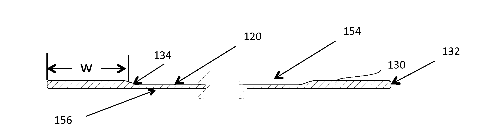
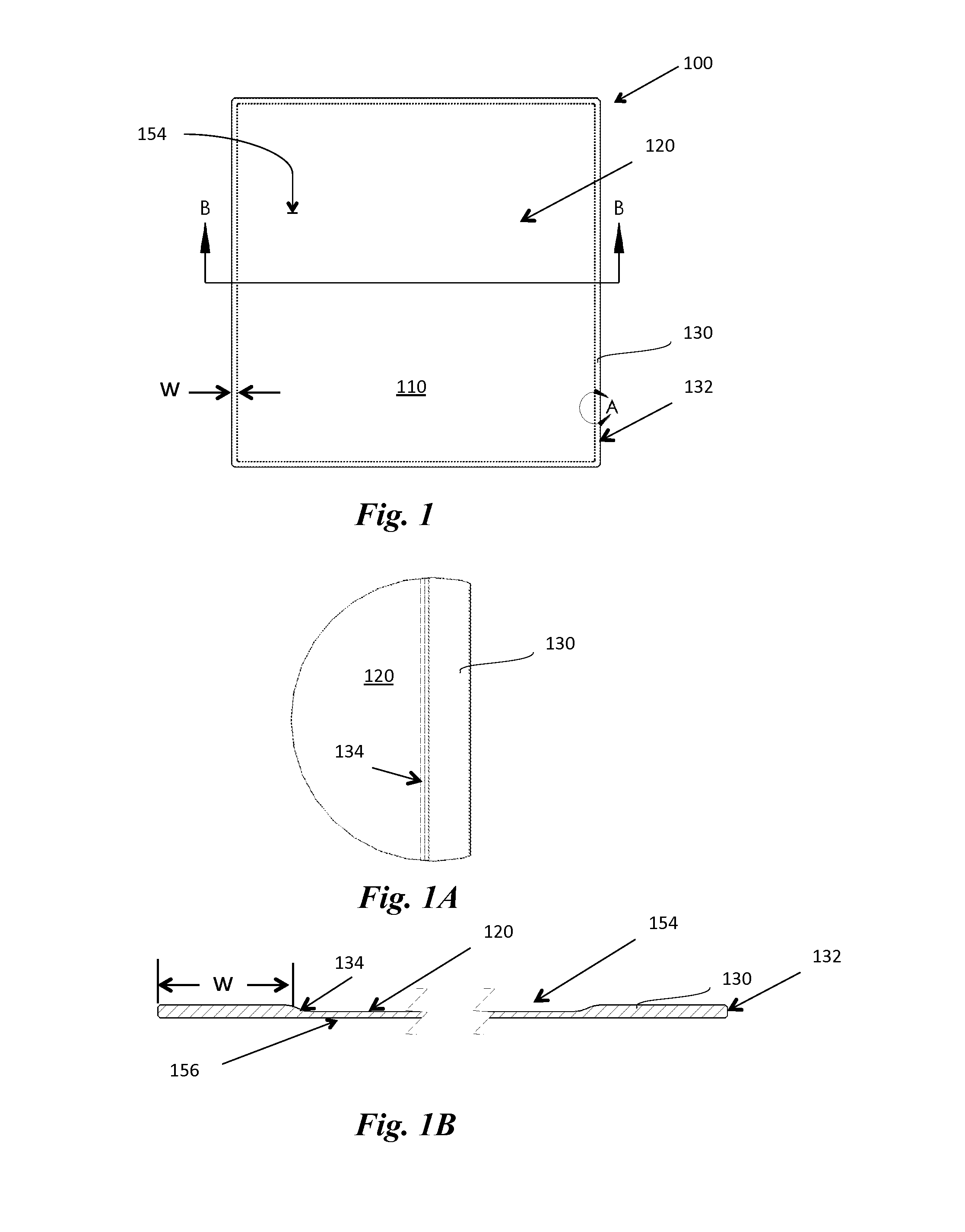
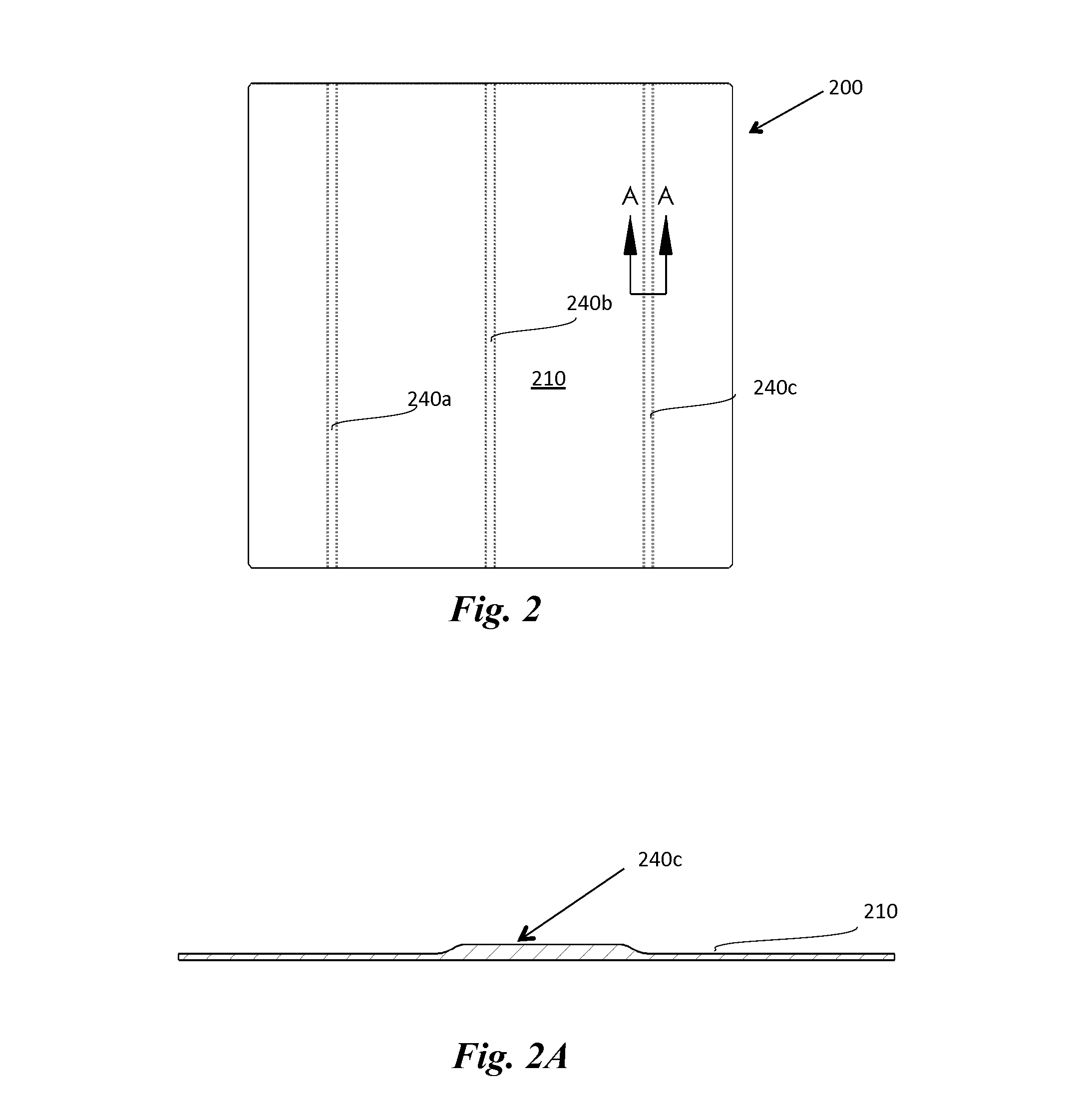
[0090]Inventions disclosed herein relate to semi-conductor wafers and methods of forming such wafers. They are particularly applicable to semi-conductor wafers for use in photovoltaic assemblies, and methods of fabricating such wafers and such assemblies, although they can be used for formation of wafer-like articles for other uses. Silicon wafers are discussed as an example, but the inventions are not limited to silicon as the semi-conductor. Similarly, although photovoltaic uses are discussed as exemplary, the methods disclosed herein can be used with any semi-conductor article manufactured from a volume of molten material, using a porous body such as a template described herein where it is desired to have regions that are thinner than others, which are thicker, and also, in particular, where the thin regions are quite thin, and are strengthened to some extent by presence of the thickened regions.

[0091]As discussed above, inventions disclosed herein can relate in general to wafers...


PUM

PropertyMeasurementUnit
thicknessaaaaaaaaaa
thicknessaaaaaaaaaa
thicknessaaaaaaaaaa

Abstract

Semi-conductor wafers with thin and thicker regions at controlled locations may be for Photovoltaics. The interior may be less than 180 microns or thinner, to 50 microns, with a thicker portion, at 180-250 microns. Thin wafers have higher efficiency. A thicker perimeter provides handling strength. Thicker stripes, landings and islands are for metallization coupling. Wafers may be made directly from a melt upon a template with regions of different heat extraction propensity arranged to correspond to locations of relative thicknesses. Interstitial oxygen is less than 6×10¹⁷ atoms / cc, preferably less than 2×10¹⁷, total oxygen less than 8.75×10¹⁷ atoms / cc, preferably less than 5.25×10¹⁷. Thicker regions form adjacent template regions having relatively higher heat extraction propensity; thinner regions adjacent regions with lesser extraction propensity. Thicker template regions have higher extraction propensity. Functional materials upon the template also have differing extraction propensities.

Description

RELATED DOCUMENTS[0001]This application claims priority to U.S. Provisional application No. 61 / 986,388, filed on Apr. 30, 2014, entitled METHODS AND APPARATI FOR THE AUTOMATED MANUFACTURE OF KERFLESS WAFERS, and also claims priority to U.S. Provisional application No. 62 / 011,866, filed on Jun. 13, 2014, entitled TECHNIQUES, METHODS AND APPARATI FOR THE AUTOMATED MANUFACTURE OF KERFLESS WAFERS. Both of the above mentioned applications are incorporated herein fully by reference.BACKGROUND[0002]Typically, silicon wafers for solar cells are 156 mm×156 mm and 180 to 200 microns thick. Because the highly refined silicon used to make these wafers is quite expensive, it would be advantageous to use thinner wafers, in order to reduce materials costs. Further, with an appropriate cell construction, the relatively thinner silicon wafers have relatively higher efficiency than thicker silicon cells. Cell constructions that would show higher efficiency using thinner wafers are those that result i...

Claims


Application Information

Patent Timeline
Patent Type & Authority Applications(United States)
IPC IPC(8): C30B11/02C30B29/06H01L29/06
CPCC30B11/02H01L31/035281C30B29/06H01L29/0657H01L31/022441H01L31/028H01L31/0682H01L31/1804Y02E10/547Y02P70/50Y02E10/50
Inventor SACHS, EMANUEL M.JONCZYK, RALFLORENZ, ADAM L.WALLACE, RICHARD L.HUDELSON, G.D. STEPHEN
Owner CUBICPV INC
Why Eureka
Try Eureka