Method and apparatus for generating a layout for a transistor

a transistor and layout technology, applied in the direction of instrumentation, program control, cad circuit design, etc., can solve the problems of ic designers' inability to meet the requirements of a transistor layout, the size of device features presently being fabricated on ic chips is smaller, and the shape of a feature is different from the intended shap

Active Publication Date: 2011-04-12
SYNOPSYS INC
View PDF21 Cites 107 Cited by
  • Summary
  • Abstract
  • Description
  • Claims
  • Application Information

AI Technical Summary

Problems solved by technology

However, nanometer-scale semiconductor fabrication technologies present a number of challenges to IC designers.
One problem is that the sizes of device features, which are presently being fabricated on IC chips are smaller than the wavelength of light used to expose the features on the IC chip.
As a result, optical effects, such as interference and fringing, can cause the shape of a feature to be different than the intended shape of the feature.
These non-uniform fabricated transistor gate shapes can cause the transistor to exhibit undesirable operating characteristics such as current crowding, excessive leakage currents, and overheating.
Unfortunately, even if the fabricated transistor gate shape is substantially rectangular, transistors with smaller feature sizes tend to have a non-uniform threshold voltage distribution and a non-uniform current density across the transistor channel.
As a result, the transistor's operating characteristics can be a non-linear function of channel width W, thereby complicating the task of designing circuits.

Method used


Image

  • Method and apparatus for generating a layout for a transistor
  • Method and apparatus for generating a layout for a transistor
  • Method and apparatus for generating a layout for a transistor

Examples


Embodiment Construction

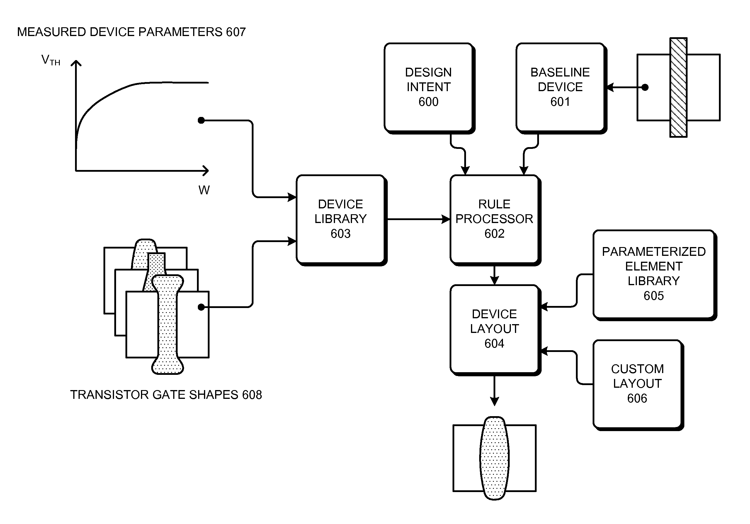
[0023]The following description is presented to enable any person skilled in the art to make and use the invention, and is provided in the context of a particular application and its requirements. Various modifications to the disclosed embodiments will be readily apparent to those skilled in the art, and the general principles defined herein may be applied to other embodiments and applications without departing from the spirit and scope of the present invention. Thus, the present invention is not limited to the embodiments shown, but is to be accorded the widest scope consistent with the principles and features disclosed herein.

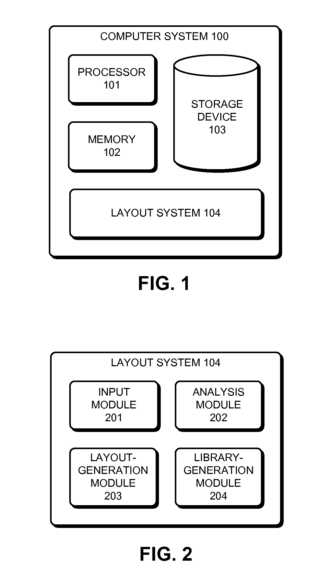
[0024]The data structures and code described in this detailed description are typically stored on a computer-readable storage medium, which may be any device or medium that can store code and / or data for use by a computer system. This includes, but is not limited to, volatile memory, non-volatile memory, magnetic and optical storage devices such as disk drive...


PUM


Abstract

A system that generates a layout for a transistor is presented. During operation, the system receives a transistor library which includes operating characteristics of fabricated transistors correlated to transistor gate shapes. The system also receives one or more desired operating characteristics for the transistor. Next, the system determines a transistor gate shape for the transistor based on the transistor library so that a fabricated transistor with the transistor gate shape substantially achieves the one or more desired operating characteristics. The system then generates the layout for the transistor which includes the transistor gate shape.

Description

BACKGROUND[0001]1. Field of the Invention[0002]The present invention relates to techniques for generating a layout for a transistor. More specifically, the present invention relates to a method and apparatus for generating a layout for a transistor so that a transistor which is fabricated from the layout achieves one or more desired operating characteristics.[0003]2. Related Art[0004]Nanometer-scale semiconductor fabrication technologies make it possible to fabricate a large number of transistors on an integrated circuit (IC) chip. As a result, the performance and functionality of IC chips has increased while the cost of individual transistors on the IC chips has decreased. However, nanometer-scale semiconductor fabrication technologies present a number of challenges to IC designers.[0005]One problem is that the sizes of device features, which are presently being fabricated on IC chips are smaller than the wavelength of light used to expose the features on the IC chip. As a result, ...

Claims


Application Information

Patent Timeline
Patent Type & Authority Patents(United States)
IPC IPC(8): G06F17/50G06F9/45
CPCG06F17/5068G06F30/39
Inventor MOROZ, VICTORLIN, XI-WEIRUBIN, MARK
Owner SYNOPSYS INC
Why Eureka
Try Eureka