Eureka AIR delivers breakthrough ideas for toughest innovation challenges, trusted by R&D personnel around the world.

Contact probe pin

a technology of contact probe and contact pin, which is applied in the direction of coupling device connection, instruments, manufacturing tools, etc., can solve the problems of deterioration in some cases of low adhesion to the device under test, tin contained therein, and a property inherent in the carbon film, so as to improve the electrical conductivity of the carbon film, improve the contact resistance value, and improve the effect of durability

Active Publication Date: 2011-05-03
KOBE STEEL LTD +1
View PDF9 Cites 12 Cited by
  • Summary
  • Abstract
  • Description
  • Claims
  • Application Information

AI Technical Summary

Benefits of technology

[0010]The present invention has been made under these circumstances, and an object of the present invention is to provide a contact probe pin having both electrical conductivity and durability and being capable of realizing low adhesion to the device under test (particularly, tin contained therein) and thereby stably maintaining electrical contact over a long period of time.
[0020]In the contact probe pin of the present invent, the content of the metal and / or a carbide thereof in the carbon film is set to differ between the tip part allowed to come into contact with the device under test during testing and the lateral part being not in contact with the device under test during testing, and the content of the metal or a carbide thereof in the tip part having the greatest contribution to the electrical contact is made larger than the content thereof in other portions, so that not only good electrical conductivity in the tip part but also low adhesion to the device under test (particularly tin contained therein) in other portions can be ensured and electrical contact can be stably maintained over a long period of time.

Problems solved by technology

More specifically, in the conventionally proposed techniques, a predetermined amount of a metal is contained so as to improve the electrical conductivity of the carbon film, but when the amount of such a metal (or a carbide thereof) is increased, the low adhesion to the device under test (particularly, tin contained therein), which is a property inherent in the carbon film, is rather deteriorated in some cases.

Method used


Image

  • Contact probe pin
  • Contact probe pin
  • Contact probe pin

Examples


example 1

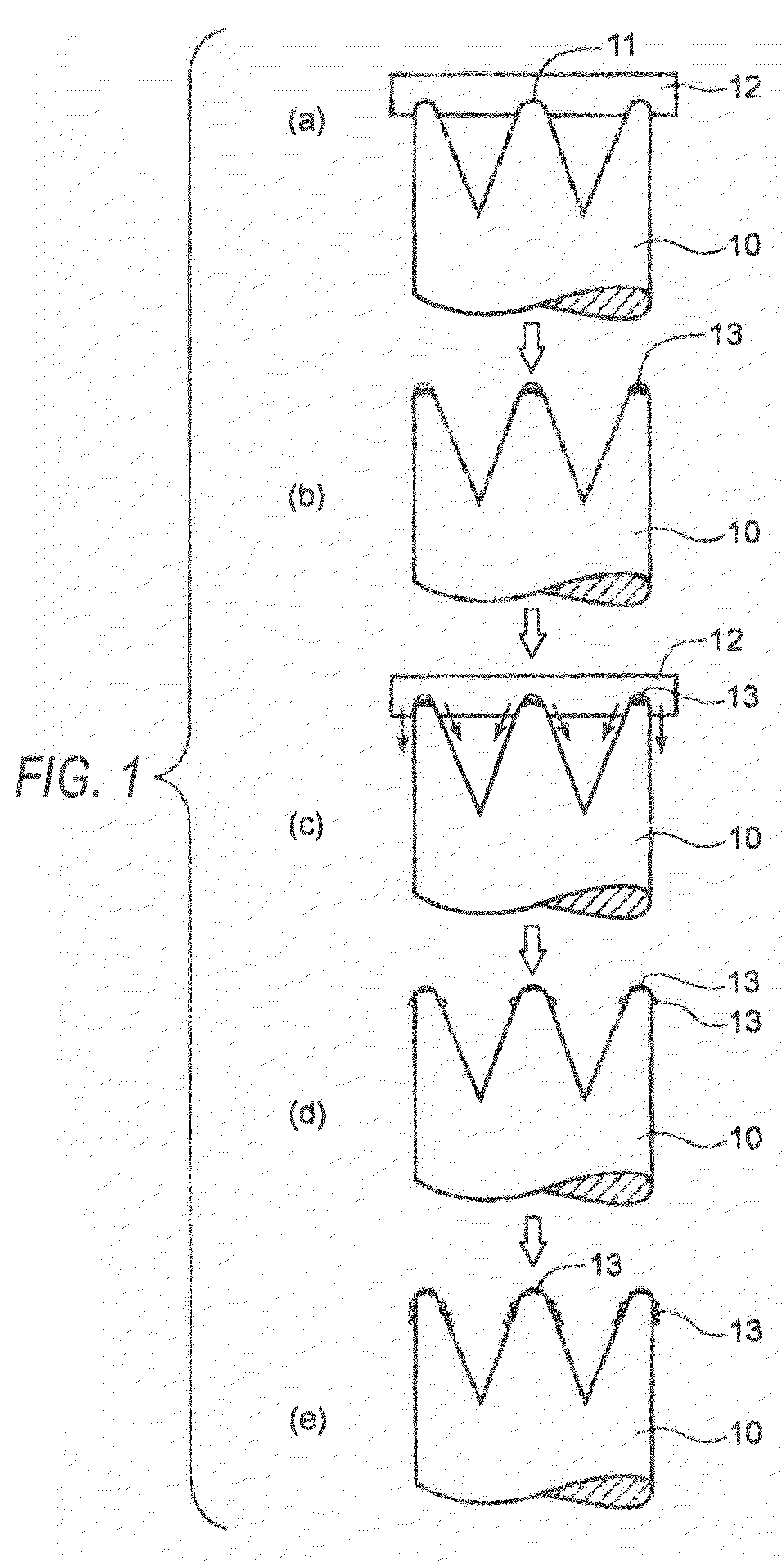
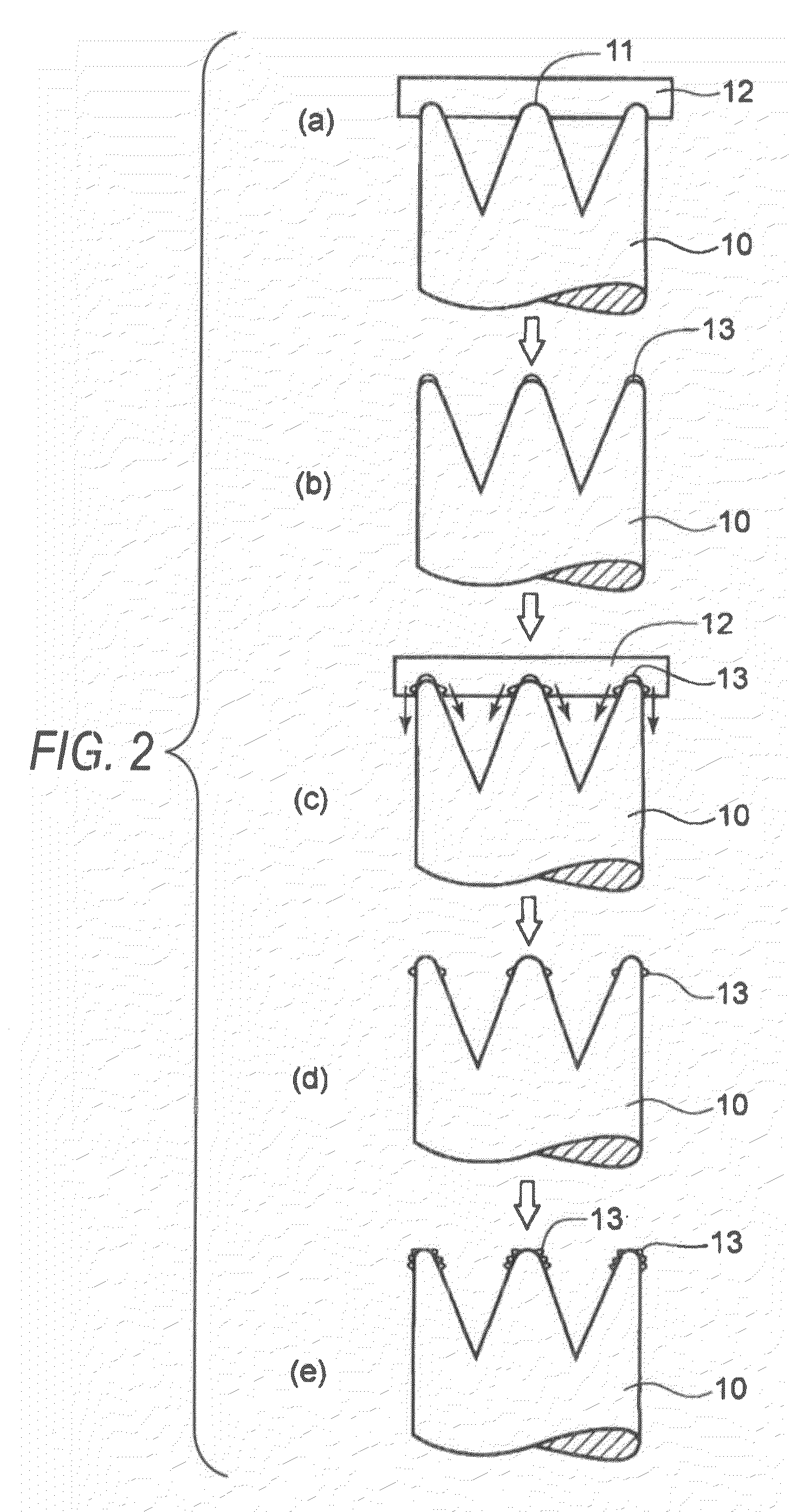
[0054]A spring-containing contact probe pin with the tip part being divided in quarters similarly to those shown in FIGS. 1(a) to 1(e) and FIGS. 2(a) to 2(e) was used. A metal was doped into carbon film, and in order to control the concentration distribution of the metal, the following method was further employed.

[0055]In a parallel plate-type magnetron sputtering apparatus (manufactured by Shimadzu Corporation), a carbon (graphite) target and a chromium target were disposed, and a base material (made of Be—Cu) of the contact probe pin was disposed by arranging its tip part to face the targets (disposed such that the axial core direction of the base material runs perpendicularly to the target face). At this time, for allowing the carbon film to be formed only in a region of about 0.3 mm from the tip part toward the basal part of the contact probe pin, the portion other than that was masked with a jig. Also, the distance between the tip part of the base material and the target was se...

example 2

[0065]A carbon film was formed under the same conditions as in Example 1 except for changing the bias voltage to −100 V and analyzed for the composition (atomic %) at each position in the same manner.

(Results of Composition Analysis)

[0066]Tip part: C: 73.0, Ar: 4.1, W: 22.9

[0067]Lateral part (position at 10 μm, outer peripheral surface): C: 76.1, Ar: 4.1, W: 19.8

[0068]Lateral part (position at 10 μm, inner peripheral surface): C: 78.78, Ar: 3.57, W: 17.65

[0069]Lateral part (position at 20 μm, outer peripheral surface): C: 77.4, Ar: 3.7, W: 18.9

[0070]Using the contact probe pin having formed thereon the carbon film as above (Examples 1 and 2), a contact energization test was performed 100,000 times on an electrode composed of a lead-free solder (Sn+3 atomic % Cu+0.5 atomic % Ag), as a result, it was confirmed that the contact probe pin exhibits excellent resistance stability as compared with the conventional contact probe pin (Au-plated product).

example 3

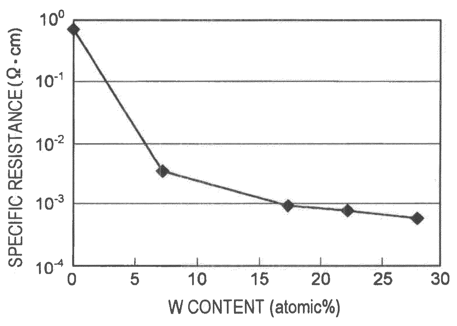
[0075]The relationship between the content of W in the carbon film and the electric resistance (specific resistance) was examined. At this time, as a specimen, a carbon film (thickness: 0.5 μm) was formed on an insulating substrate by variously changing the content of W (the content was measured by EPMA), and the specific resistance of each carbon film was measured by the following method.

(Method for Measuring Specific Resistance)

[0076]The sheet resistance of the thin film was measured using a commercially available measuring instrument (3226 mΩ HI TESTER manufactured by Hioki E. E. Corporation+a four-probe measuring device manufactured by Kyowa Riken Ltd.) according to a four probe method generally employed in the measurement of resistance of a thin film, and the specific resistance was calculated by multiplying the measured value by the film thickness and a correction factor for sheet resistance (=4.532).

[0077]The results (the relationship between the content of W and the specific...


PUM

PropertyMeasurementUnit
contact resistanceaaaaaaaaaa
thicknessaaaaaaaaaa
thicknessaaaaaaaaaa

Abstract

The present invention provides a contact probe pin having both electrical conductivity and durability and being capable of realizing low adhesion to the device under test (particularly, tin contained therein) and thereby stably maintaining electrical contact over a long period of time. The present invention relates to a contact probe pin comprising: a base material; and a carbon film comprising at least one of a metal and a carbide thereof, wherein the carbon film is continuously formed over the surface of from a tip part of the contact probe pin to a lateral part of the contact probe pin, and a content of the at least one of a metal and a carbide thereof in the carbon film is continuously or intermittently decreased from the tip part toward the lateral part.

Description

CROSS-REFERENCE TO RELATED APPLICATIONS[0001]This application claims priority from Japanese Patent Application No. 2009-185271 filed on Aug. 7, 2009, the entire subject matter of which is incorporated herein by reference.BACKGROUND OF THE INVENTION[0002]1. Field of the Invention[0003]The present invention relates to a contact probe pin used for testing electrical properties of a semiconductor device. More specifically, the present invention relates to a contact probe pin having durability high enough not to deteriorate in the electrical conductivity even by the repetition of the test.[0004]2. Description of the Related Art[0005]An electronic component such as integrated circuit (IC), large-scale integrated circuit (LSI) and light emitting diode (LED) (that is, an electronic component using a semiconductor device) is tested for its electrical properties by contacting a probe pin with the electrode of the semiconductor device. The probe pin (contact probe pin) used in such a testing a...

Claims


Application Information

Patent Timeline
Patent Type & Authority Patents(United States)
IPC IPC(8): B23B9/00
CPCG01R1/06738H01R13/22H01R13/03Y10T428/30G01R1/06761
Inventor HIRANO, TAKAYUKIMIYAMOTO, TAKASHI
Owner KOBE STEEL LTD
Why Eureka
Eureka Blog
Learn More