Marking method and sheet for both protective film forming and dicing

a marking method and protective film technology, applied in the direction of film/foil adhesives, manufacturing tools, semiconductor/solid-state device details, etc., can solve the problems of uneven quality, difficulty in dripping the proper amount of resin, and additional equipment and operation costs, and achieve high accuracy

Active Publication Date: 2011-05-03
LINTEC CORP
View PDF10 Cites 34 Cited by
  • Summary
  • Abstract
  • Description
  • Claims
  • Application Information

AI Technical Summary

Benefits of technology

[0028]According to the invention, in the process in which the marking is performed on the protective film formed on the work, the marking method in which the marking is performed on the protective film with a high accuracy by suppressing the warpage of the work and, also, the sheet for both protective film forming and dicing which is advantageously used in the method are provided.

Problems solved by technology

The potting method has a drawback of difficulty in dripping the proper amount of the resin.
The molding method involves washing of the mold, which will require additional costs for equipment and operation thereof.
Such resin coating may cause uneven quality because of difficulty in spreading a proper amount of resin uniformly on the chip.
The minute scratches may cause cracks during the dicing in the step (3) or after the device is packaged.
The chemical etching, as a matter of course, raises problems related to the cost increase for its equipment and operation.
In the above-described process, there has been a case in which, when the sheet for the protective film forming layer for chips is adhered to the wafer, tension applied to the sheet remains after it is adhered to cause the wafer to have a warpage.

Method used


Image

  • Marking method and sheet for both protective film forming and dicing
  • Marking method and sheet for both protective film forming and dicing
  • Marking method and sheet for both protective film forming and dicing

Examples


example 1

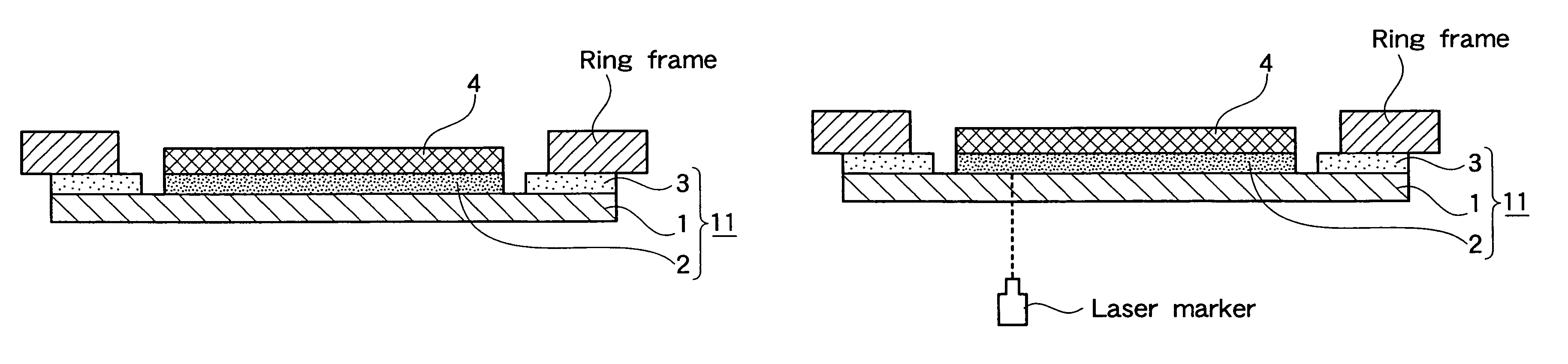
[0130]A sheet for both protective film forming and dicing having a constitution as shown in FIG. 1 was prepared in a manner as described below.

[0131]A composition for a protective film forming layer was coated on one face of the support film “A” on which a release treatment was performed such that a thickness thereof after removal of a solvent being 50 μm and, then, dried and, thereafter, a release film (trade name: SP-PET 3811; available from Lintec Corporation) was laminated on the face of the protective film forming layer, to obtain a protective film forming layer having a support film.

[0132]The adhesive “A” was coated on one face of a PET film (thickness: 25 μm) such that a thickness after removal of a solvent being 10 μm and, then, dried and, thereafter, a release film (trade name: SP-PET3811) was laminated on the face of the adhesive “A”. Further, the adhesive B was coated on the opposite face of the PET film so that the thickness after the removal of the solvent is 10 μm and ...

example 2

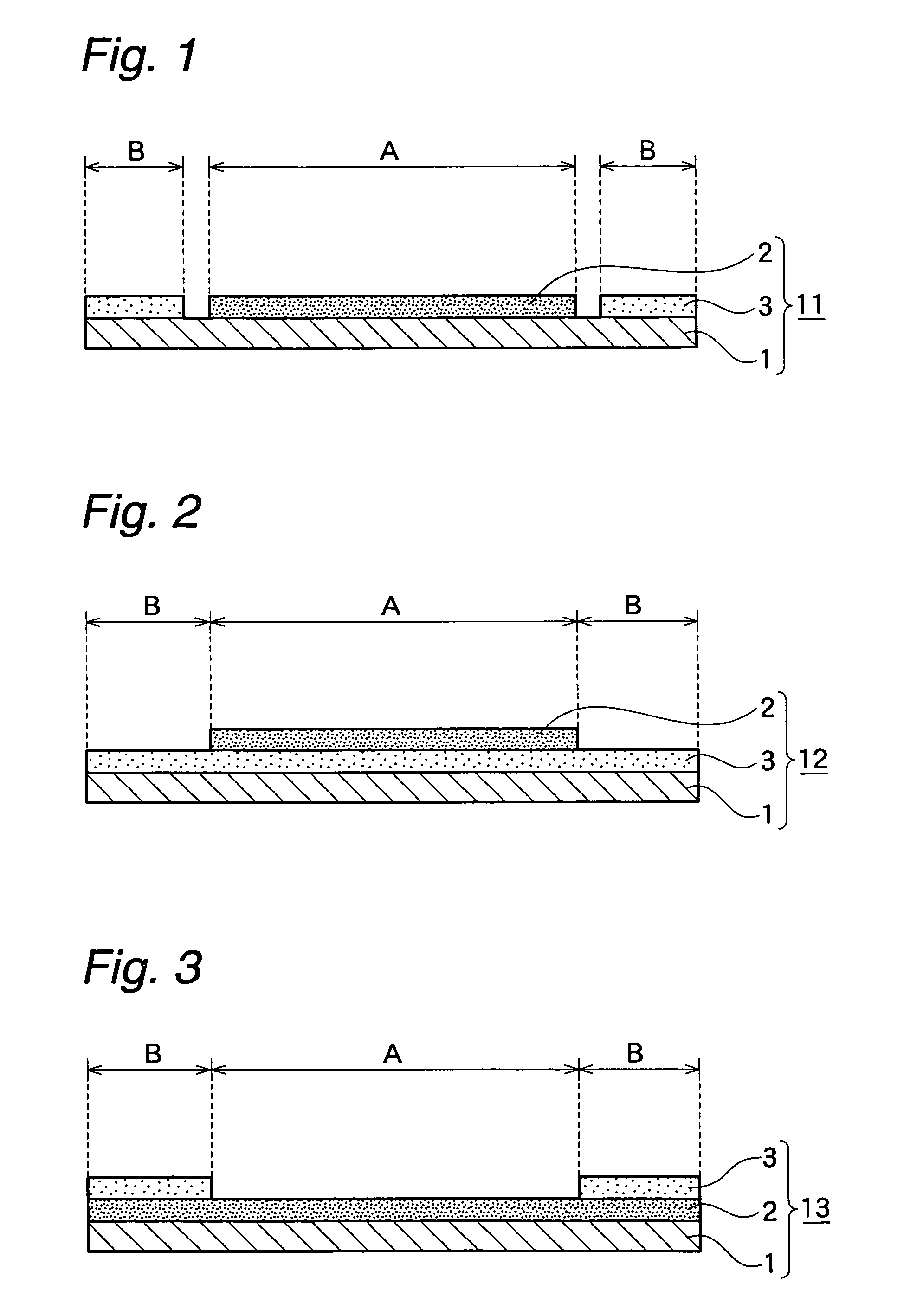
[0135]A sheet for both protective film forming and dicing having a constitution as shown in FIG. 2 was prepared by a method as described below.

[0136]A composition for the protective film forming layer was coated on a release face of a release film (SP-PET3811) such that a thickness after removal of a solvent being 50 μm and, then, dried and, then, another release film (trade name: SP-PET3801; available from Lintec Corporation) was laminated on an exposed face of the protective film forming layer.

[0137]All layers of the protective film forming layer in which the release film was laminated on each face were cut to be in a size having a diameter of 165 mm, to thereby obtain the protective film forming layer in a circular shape. The release film on the support film B having a removable adhesive material and the release film on one face of the protective film forming layer were released therefrom and, then, the thus-exposed adhesive face and protective film forming layer were laminated o...

example 3

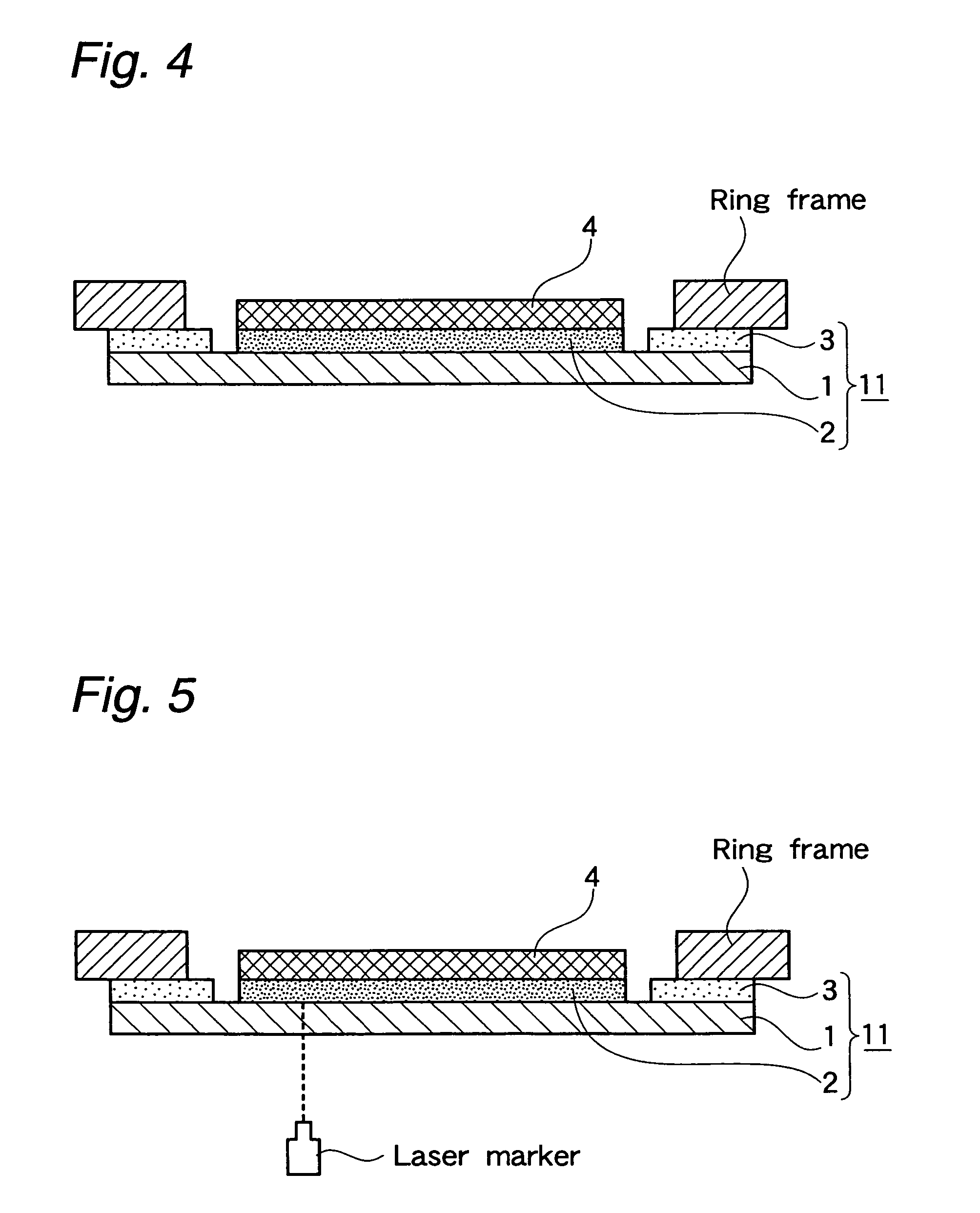
[0139]A sheet for both protective film forming and dicing having a constitution as shown in FIG. 3 was prepared by a method as described below.

[0140]A composition for the protective film forming layer was coated on a release-treated face of a support film “C” such that a thickness after removal of a solvent being 50 μm and, then, dried and, then, a release film (SP-PET3811) was laminated on a face of the protective film forming layer, to thereby obtain a protective film forming layer having a support film.

[0141]The adhesive “A” was applied on a release face of the release film (SP-PET3811) such that a thickness after removal of a solvent being 20 μm and, then, dried and, thereafter, another release film (SP-PET3801) was laminated on the exposed adhesive face. The resultant laminate was allowed to be a double-face adhesive sheet without carrier which was, then, used as a removable adhesive material. The removable adhesive material was die-cut to be in a size having a diameter of 165 ...


PUM

PropertyMeasurementUnit
distanceaaaaaaaaaa
melting pointaaaaaaaaaa

Abstract

The invention provides a marking method in which marking is performed on a protective film formed on a work with a high accuracy while suppressing a warpage and, also, a sheet for both protective film forming and dicing which is advantageously used in the method. The marking method comprises irradiating laser light to a laminated structure comprising a support film tensely supported by a ring frame, a protective film releasably laminated on the support film and a work fixed to the protective film, wherein the protective film is irradiated laser light from a side of the support film, to thereby mark the protective film.

Description

BACKGROUND OF THE INVENTION[0001]1. Field of the Invention[0002]The present invention relates to a method for forming a protective film and, then, performing marking on the protective film, and a sheet for both protective film forming and dicing which is favorably used in the method.[0003]2. Description of the Prior Art[0004]Recently, production of semiconductor devices is made through a so-called face down mounting process. In the face down process, chips are electrically connected with a substrate through a convex portion called as a bump formed on a circuit surface of the chip to ensure its conductivity to the substrate.[0005]Semiconductor devices are generally produced though the following steps:[0006](1) forming a circuit on a surface of a wafer by etching or the like and providing a bump on a given position of the circuit surface;[0007](2) grinding a back surface of the wafer to have a given thickness;[0008](3) fixing the back surface of the wafer onto a dicing sheet which is ...

Claims


Application Information

Patent Timeline
Patent Type & Authority Patents(United States)
IPC IPC(8): H01L21/00B23K26/00H01L23/00
CPCH01L21/67092H01L21/67132H01L21/67282H01L21/6836H01L23/544H01L24/27H01L24/29H01L24/83H01L2924/01029H01L21/78H01L2221/68327H01L2223/54473H01L2223/54486H01L2224/83191H01L2924/3512H01L2924/00H01L2924/181H01L2224/94H01L2224/27C09J7/22C09J7/29C09J7/40C09J7/30C09J7/38B23K26/0006B23K2103/00C09J2203/326
Inventor SAIKI, NAOYASHINODA, TOMONORIHAMASAKI, AKIE
Owner LINTEC CORP
Why Eureka
Try Eureka