Organic light emitting display device

a light-emitting display and organic technology, applied in the field can solve the problems of organic light-emitting display devices, increased production costs, and increased production costs, so as to improve the mechanical reliability of encapsulating thin films, reduce thickness, and facilitate manufacturing

Active Publication Date: 2011-05-03
SAMSUNG DISPLAY CO LTD
View PDF18 Cites 37 Cited by
  • Summary
  • Abstract
  • Description
  • Claims
  • Application Information

AI Technical Summary

Benefits of technology

[0012]It is a second object to provide an organic light emitting display device, which reduces a thickness by forming an encapsulating substrate encapsulating an organic light emitting diode with an encapsulating thin film.
[0013]It is a third object to provide an organic light emitting display device, which may improve the mechanical reliability of an encapsulating thin film by forming a protection film as the highest layer of a touch panel.
[0014]Some embodiments provide an integrated display and touch input device comprising a display, for example, an organic light emitting display, on which a set of third electrodes of the touch input device is disposed on an upper surface of the display and a set of fourth electrodes of the touch input device are disposed on an upper substrate. A spacing member defines a space between the third and fourth electrodes. In some embodiments, the third and fourth electrodes are configured such that an external pressure on the upper substrate results in contact between the third and fourth electrodes, which generates a signal that is converted into a location on the display device. Embodiments of the integrated display and touch input device are thinner and / or easier to manufacture.

Problems solved by technology

Meanwhile, when an organic light emitting display device is exposed to moisture or oxygen, the emission layer may be damaged.
Furthermore, the organic light emitting display device has a problem that it becomes thicker due to an encapsulating substrate encapsulating an organic light emitting diode and a touch panel.

Method used


Image

  • Organic light emitting display device
  • Organic light emitting display device
  • Organic light emitting display device

Examples


first embodiment

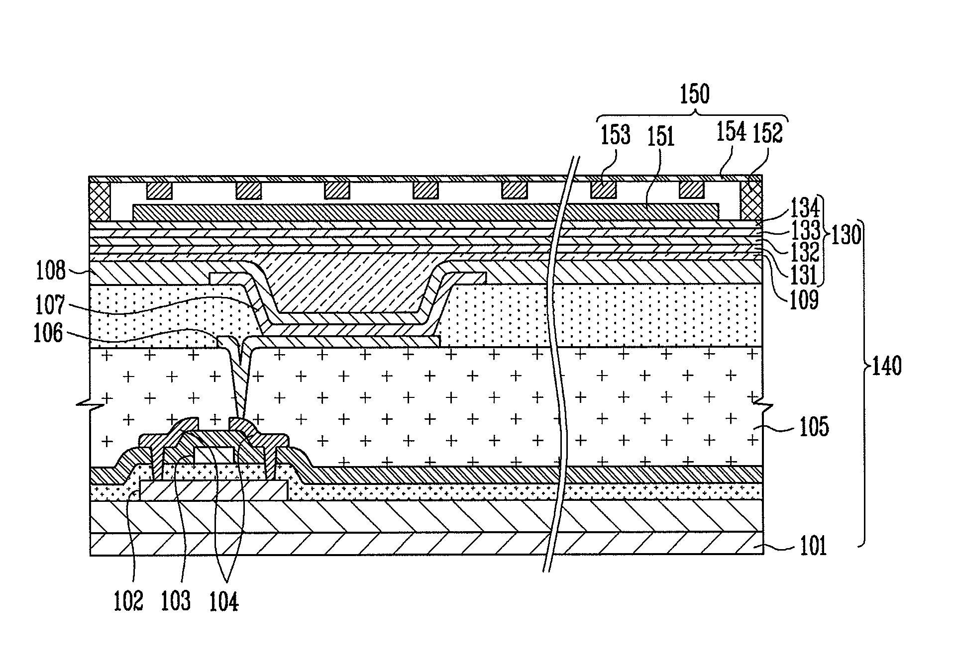
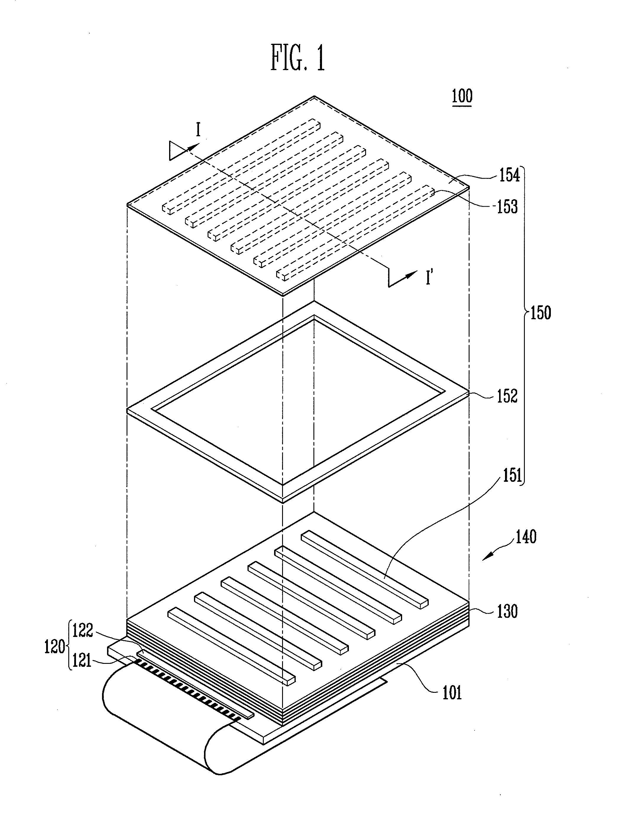
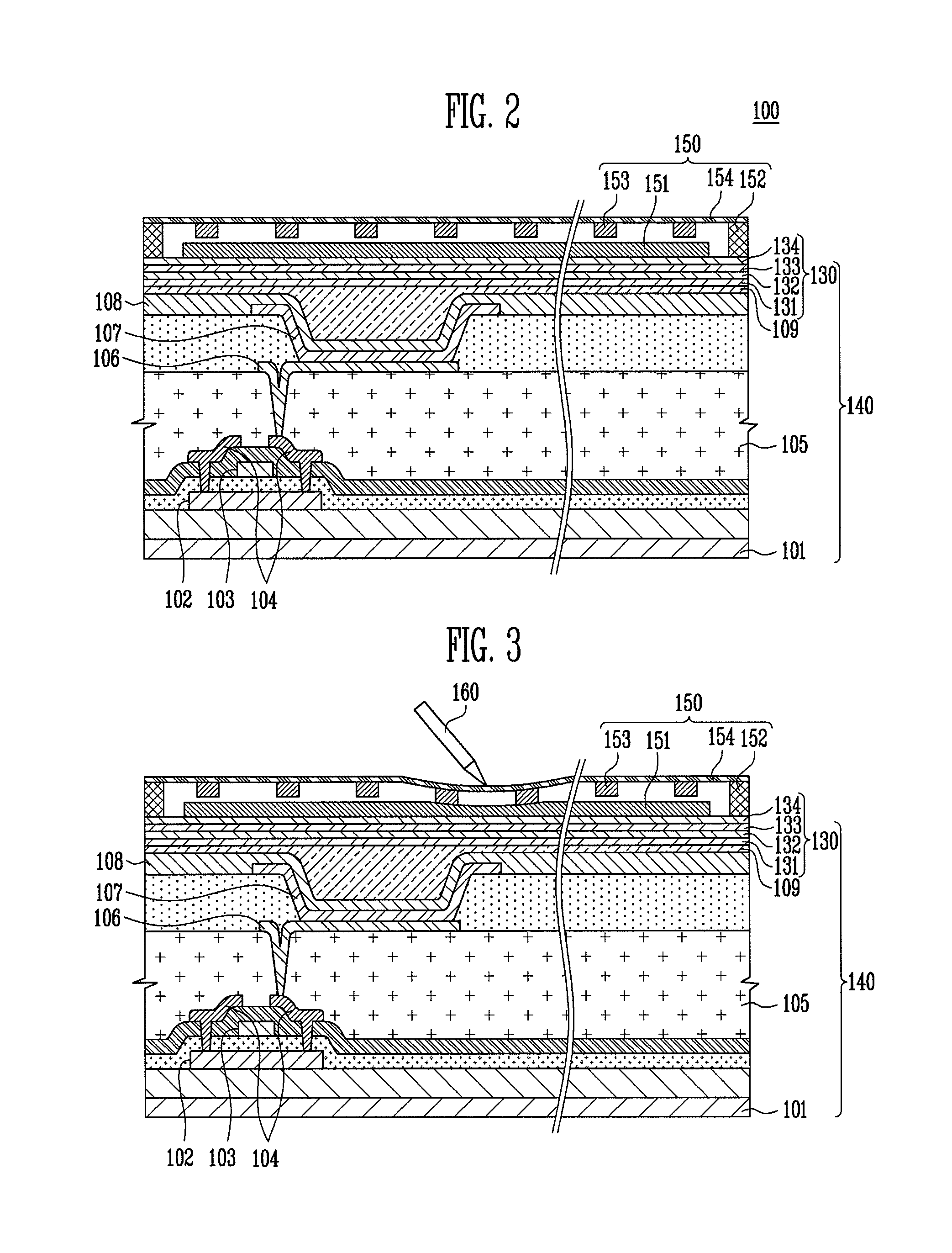
[0038]FIG. 1 is an exploded perspective view schematically showing an organic light emitting display device according to a FIG. 2 is a cross-sectional view of the organic light emitting display device taken along section line I-I′ of FIG. 1.

[0039]With reference to FIG. 1 and FIG. 2, the organic light emitting display device 100 includes a display panel 140 and an external input device 150. The display panel 140 includes a substrate 101 having at least one organic light emitting diode and an encapsulating thin film 130 for encapsulating the organic light emitting diode. The external input device 150 is formed on the display panel 140, and generates an electric signal in response to a touch operation applied from an exterior. Here, the external input device 150 includes a protection film 154 and a spacing member 152. The protection film 154 has a third electrode 151 formed on the display panel 140 and a fourth electrode 153 formed to intersect the third electrode 151. The spacing mem...

second embodiment

[0062]FIG. 5 is a perspective exploded view schematically showing an organic light emitting display device according to a FIG. 6 is a cross-sectional view of the organic light emitting display device taken along section line II-II′ of FIG. 5.

[0063]With reference to FIG. 5 and FIG. 6, the organic light emitting display device 200 includes a display panel 240 and an external input device 250. The display panel 240 includes a substrate 201 having at least one organic light emitting diode and an encapsulating thin film 230 for encapsulating the organic light emitting diode. The external input device 250 is formed on the display panel 240, and generates an electric signal in response to a touch operation applied from the exterior thereof. Here, the external input device 250 includes a protection film 254 and a spacing member 252. The external input device 250 has a third electrode 251 formed on the display panel 240 and a fourth electrode 253 formed on the protection film 254 to interse...

third embodiment

[0067]FIG. 7 is a perspective exploded view schematically showing an organic light emitting display device according to a FIG. 8 is a cross-sectional view of the organic light emitting display device taken along section line III-III′ of FIG. 7.

[0068]With reference to FIG. 7 and FIG. 8, the organic light emitting display device 300 includes a display panel 340 and an external input device 350. The display panel 340 includes a substrate 301 having at least one organic light emitting diode and an encapsulating thin film 330 for encapsulating the organic light emitting diode. The external input device 350 is formed on the display panel 340, and generates an electric signal in response to a touch operation applied from the exterior thereof. Here, the external input device 350 includes a protection film 354 and a spacing member 352. The external input device 350 has a third electrode 351 formed on the display panel 340 and a fourth electrode 353 formed to intersect the third electrode 35...


PUM

PropertyMeasurementUnit
thicknessaaaaaaaaaa
thicknessaaaaaaaaaa
pressureaaaaaaaaaa

Abstract

An organic light emitting display device having a touch panel function comprises at least one organic light emitting diode and an encapsulating thin film for encapsulating the organic light emitting diode; and an external input device formed on the display panel for generating an electric signal in response to a touch operation applied from the exterior thereof. The external input device includes an upper substrate and a spacing member. The external input device has a third electrode formed on the display panel and a fourth electrode formed on the upper substrate to intersect the third electrode. The spacing member forms a predetermined spacing between the third electrode and the fourth electrode.

Description

CROSS-REFERENCE TO RELATED APPLICATIONS[0001]This application claims the benefit of Korean Patent Application No. 10-2007-0045554, filed on May 10, 2007 in the Korean Intellectual Property Office, the entire disclosure of which is incorporated herein by reference.BACKGROUND[0002]1. Technical Field[0003]The present disclosure relates to an organic light emitting display device, more particularly to an organic light emitting display device having touch-panel functionality.[0004]2. Discussion of Related Art[0005]Recently, organic light emitting display devices have been widely used, and have relatively simple construction. Further, organic light emitting display devices can display text and graphics using an external input device. In general, an organic light emitting display device includes a first electrode, a second electrode, and at least one organic layer having an emission layer interposed between the first electrode and the second electrode. The first electrode is formed on a su...

Claims


Application Information

Patent Timeline
Patent Type & Authority Patents(United States)
IPC IPC(8): H01L51/50
CPCG06F3/0412H01L27/323G06F3/045H01L51/5253H10K59/40H10K59/873H05B33/04H05B33/26H10K50/844
Inventor KIM, HYEONG-GWON
Owner SAMSUNG DISPLAY CO LTD
Why Eureka
Try Eureka