Semiconductor chip with bond area
a technology of semiconductor and bond area, applied in the field of semiconductor chips, can solve the problems of forming multiple bumps on the chip, unable to provide the reliable bond between the chip and the substrate, and being subject to traumatized by the testing prob
- Summary
- Abstract
- Description
- Claims
- Application Information
AI Technical Summary
Benefits of technology
Problems solved by technology
Method used
Image
Examples
embodiment i
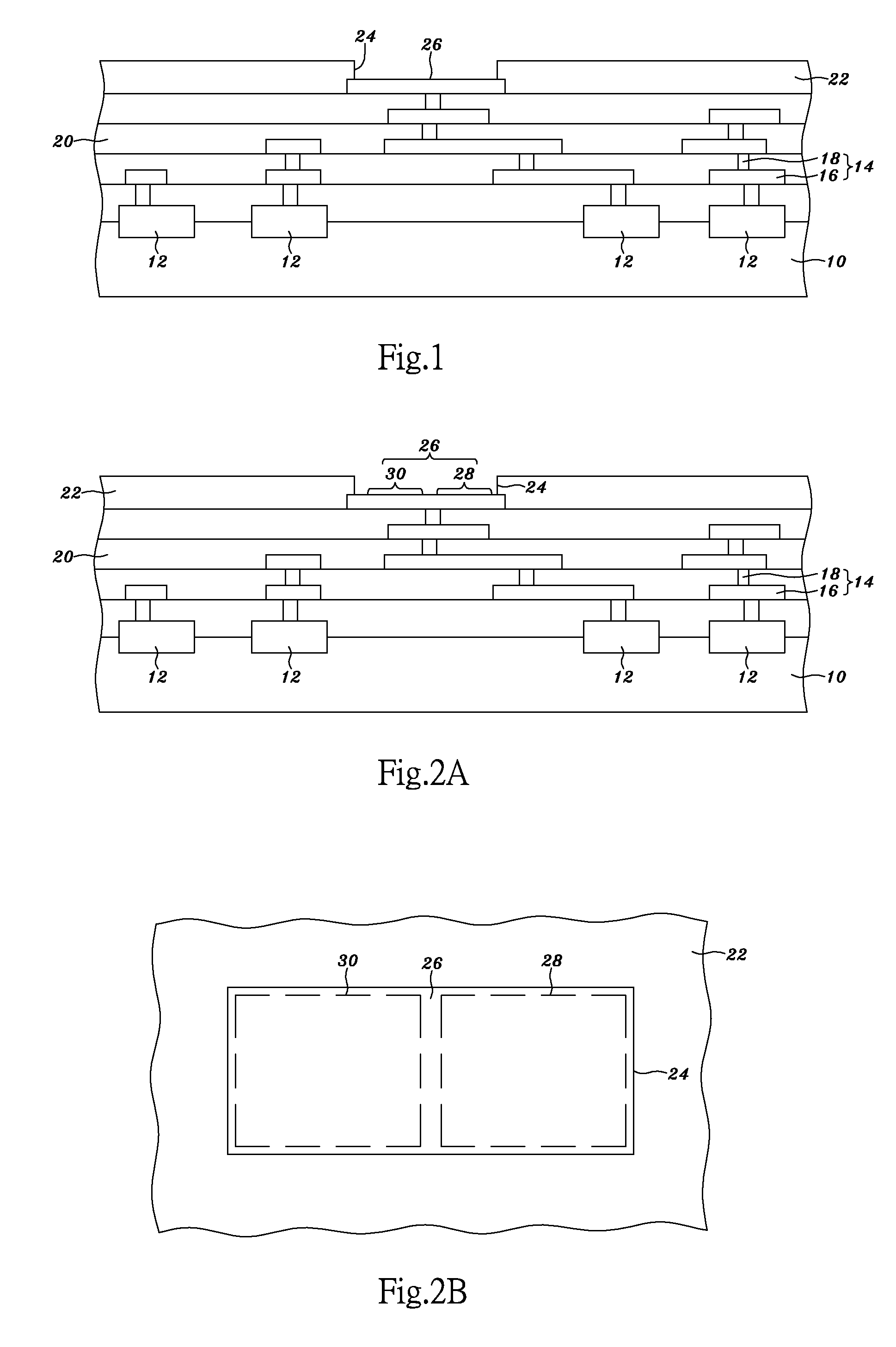
[0063]Refer to FIG. 2A and FIG. 2B respectively a sectional view and a partial top view schematically showing a wafer. As shown in FIG. 2A and FIG. 2B, the pad 26 has a testing area 28 for electrical testing and a bond area 30 to be electrically connected to an external system, such as a printed circuit board, a ball grid array (BGA) substrate, a mother board, a glass substrate, a ceramic substrate, a flexible circuit film, a TAB carrier, a semiconductor wafer, or a semiconductor chip. The examples for the external system in this embodiment may be employed to any below-mentioned external system depicted in other embodiments.
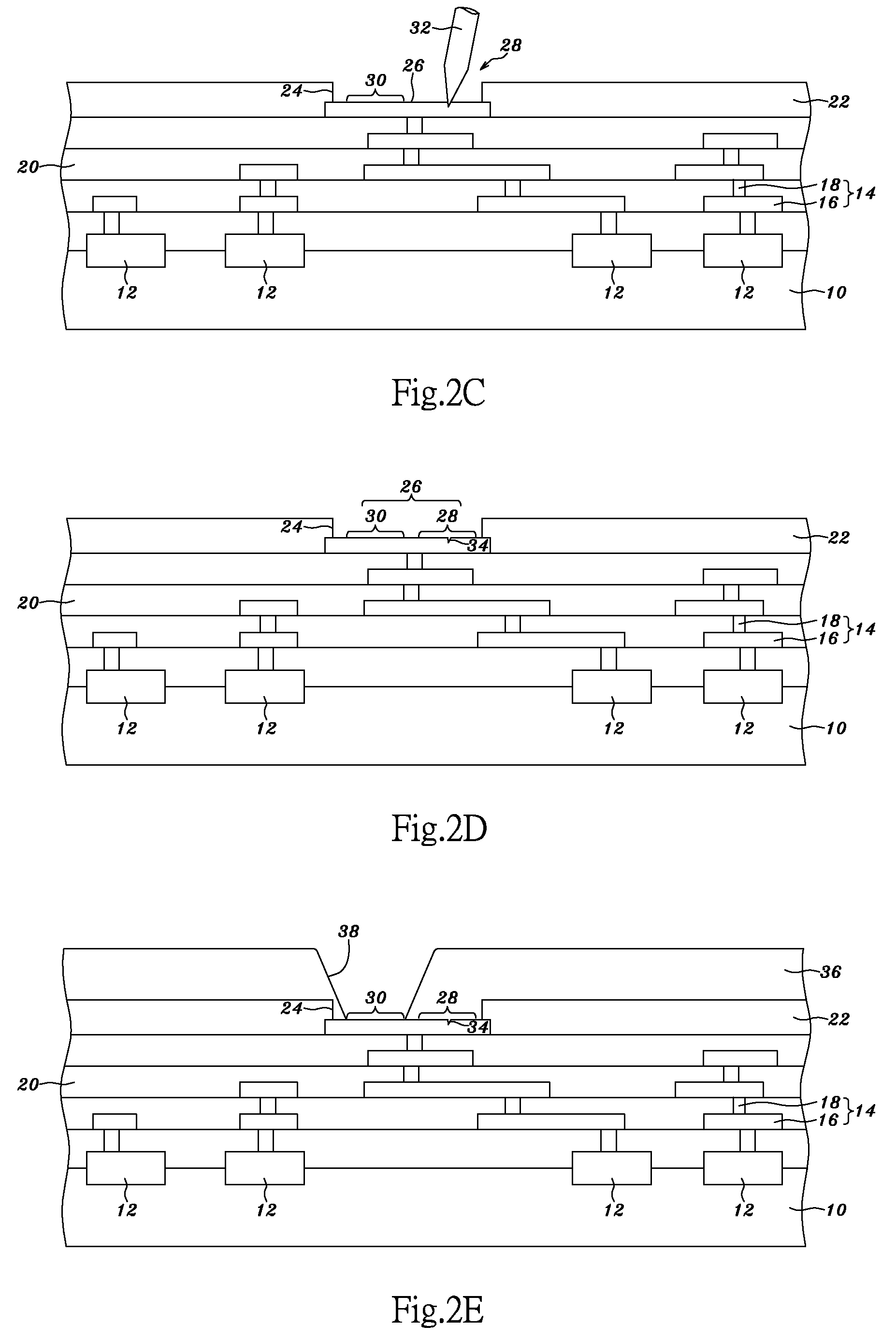
[0064]Refer to FIG. 2C. During a step of testing, a testing probe 32 contacts with the testing area 28 of a pad 26 for electrical testing. Refer to FIG. 2D. After the step of testing, the testing probe 32 is removed, and a probe mark 34 is left on the testing area 28. Refer to FIG. 2E. A patterned polymer layer 36 is formed over the passivation layer 22 and the t...
embodiment ii
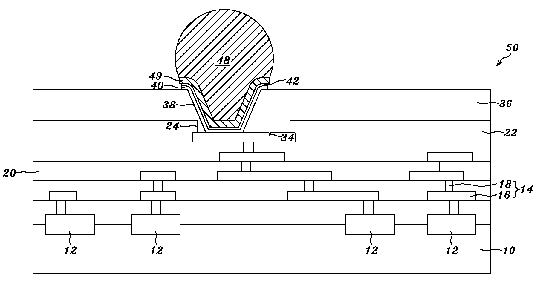
[0072]Refer to FIG. 3A. After the progress shown in FIG. 2D, an adhesion / barrier layer 40 having a thickness of between 0.02 and 2 μm is formed over the pad 26 and the passivation layer 22. Next, a seed layer 42 is formed over the adhesion / barrier layer 40. Refer to Embodiment I for the detailed technical description of the adhesion / barrier layer 40 and the seed layer 42.
[0073]Refer to FIG. 3B. Next, a photoresist layer 44 is formed over the seed layer 42, and the photoresist layer 44 is patterned to form a photoresist-layer opening 46 to expose the seed layer 42 over the bond area 30 of the pad 26, wherein a 1× stepper or a 1× scanner is used to expose the photoresist layer 44 during forming the photoresist-layer opening 46. Refer to FIG. 3C. Next, a metal layer 48 having a thickness of between 1 and 200 μm (e.g. a thickness of between 20 and 120 μm) is formed over the seed layer 42 exposed by the photoresist-layer opening 46. Refer to Embodiment I for the detailed technical descri...
embodiment iii
[0077]This embodiment exemplifies the application of the present invention to a redistribution layer (RDL). Refer to FIG. 4A. After the progress shown in FIG. 2G, a first photoresist layer 52 is formed over the seed layer 42, and the first photoresist layer 52 is patterned to form a first-photoresist-layer opening 54 to expose the seed layer 42 over the bond area 30 of the pad 26 and expose the seed layer 42 over a portion of the patterned polymer layer 36 extending from the bond area 30, wherein a 1× stepper or a 1× scanner is used to expose the first photoresist layer 52 during forming the first-photoresist-layer opening 54. The first-photoresist-layer opening 54 has a dimension W1 of between 60 μm and 10 mm.
[0078]Refer to FIG. 4B. Next, a first metal layer 56 having a thickness of between 1 and 30 μm is electroplated on the seed layer 42 exposed by the first-photoresist-layer opening 54. The first metal layer 56 may be a single layer made of gold, copper, nickel, aluminum, silver...
PUM
 Abstract
Description
Claims
Application Information


