Wafer inspection system and method thereof

a wafer inspection and inspection system technology, applied in the direction of image enhancement, semiconductor/solid-state device testing/measurement, instruments, etc., can solve the problems of difficult to apply the same objective standard to all wafers, damage to the boundary line of the pad, and inability to achieve effective electrical testing

Active Publication Date: 2005-12-22
SAMSUNG ELECTRONICS CO LTD
View PDF4 Cites 28 Cited by
  • Summary
  • Abstract
  • Description
  • Claims
  • Application Information

AI Technical Summary

Benefits of technology

[0011] In order to solve the foregoing and/or other problems, it is an aspect of the present general inventive concept to provide a wafer inspection system and a method thereof, in ...

Problems solved by technology

If the probe abnormally contacts the pad, a boundary line of the pad may be damaged, and an effective electrical test may not be expected.
Therefore, it is difficult to apply the same objective standard to all wafers because the defect is subjectively determined.
Further, it takes too much time and effort to train an inspector to obtain a reliable inspection result.
However, this conventional inspection apparatus just uses a fee...

Method used


Image

  • Wafer inspection system and method thereof
  • Wafer inspection system and method thereof
  • Wafer inspection system and method thereof

Examples


Embodiment Construction

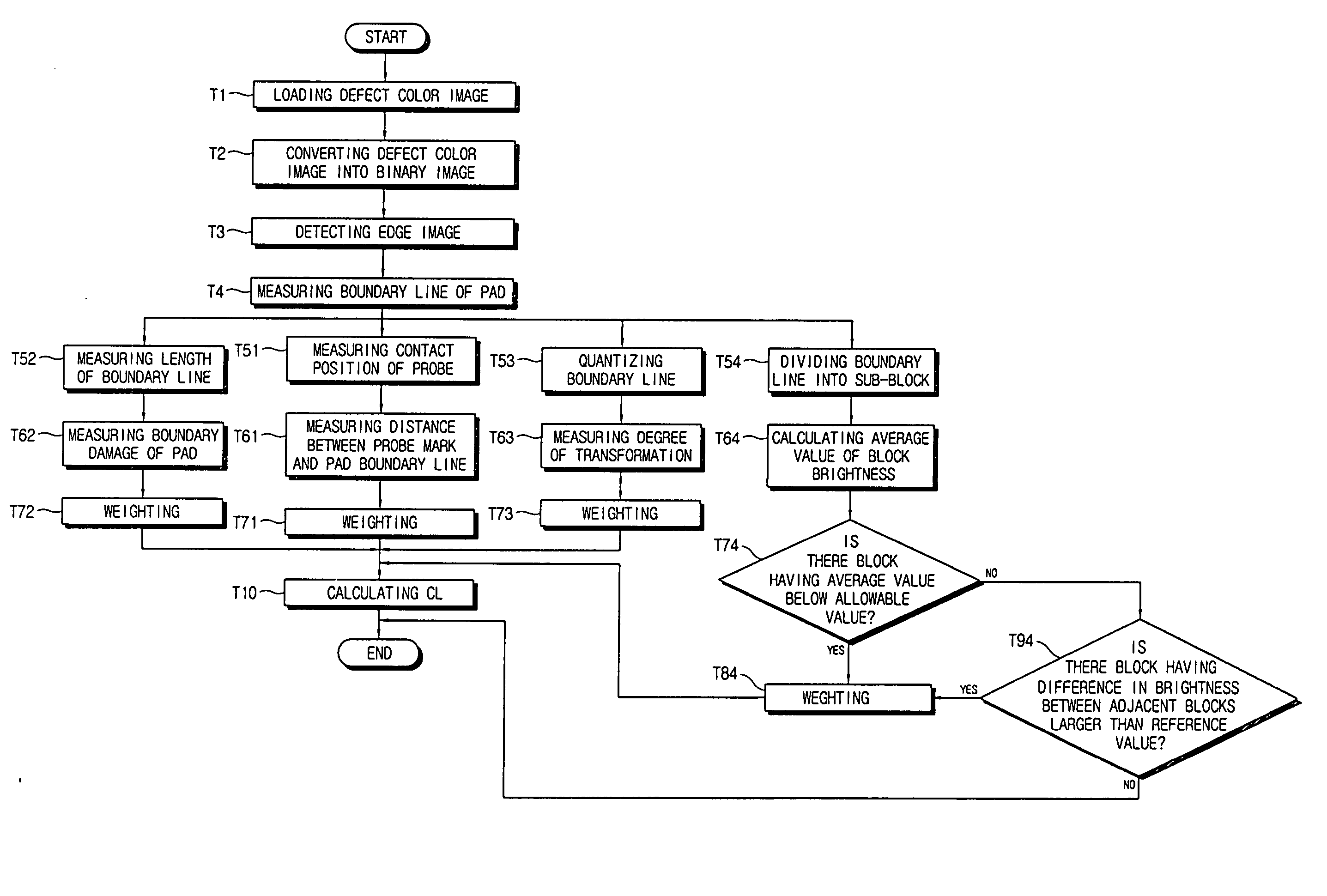
[0037] Reference will now be made in detail to the embodiments of the present general inventive concept, examples of which are illustrated in the accompanying drawings, wherein like reference numerals refer to like elements throughout. The embodiments are described below in order to explain the present general inventive concept by referring to the figures.

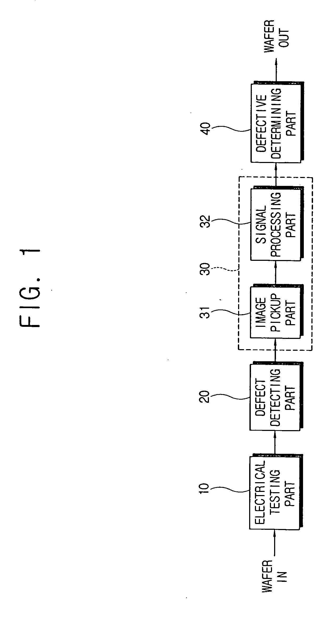
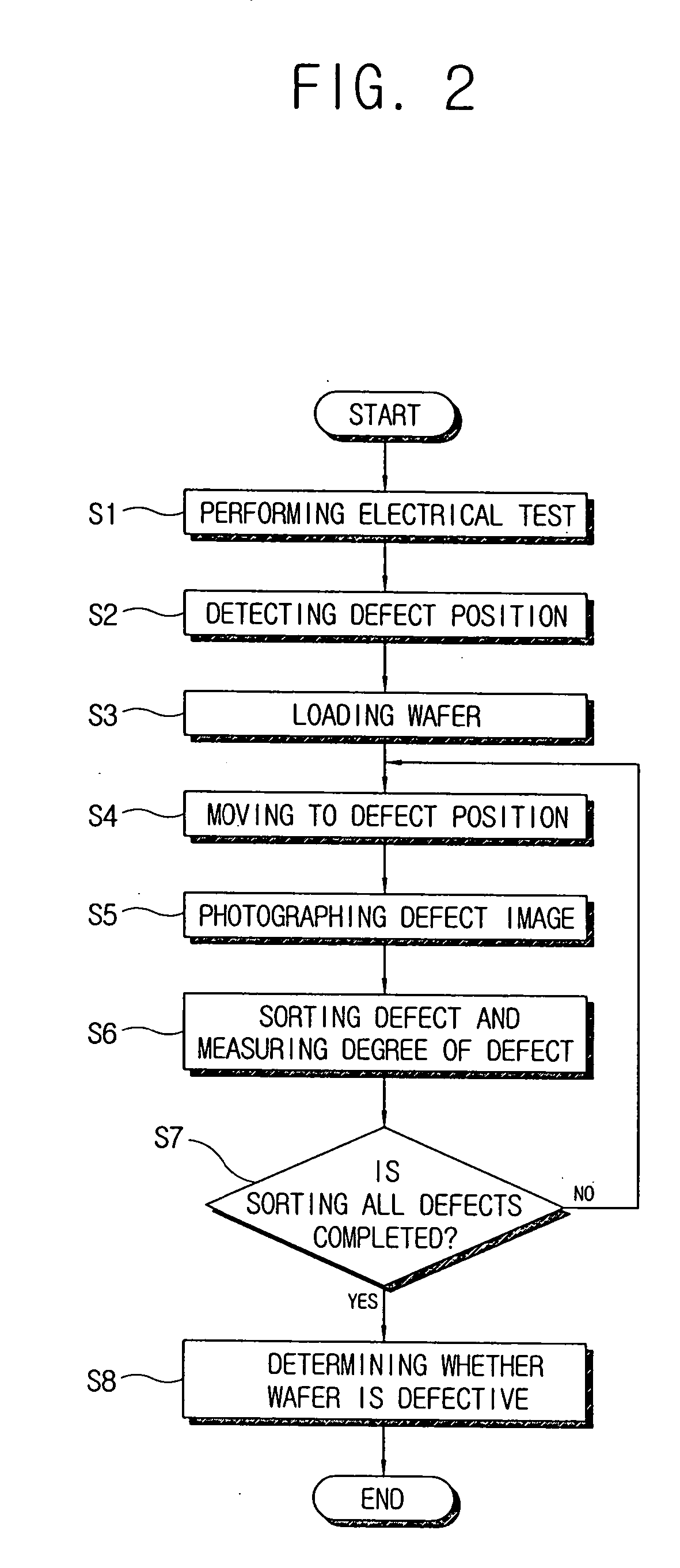
[0038] As shown in FIG. 1, a wafer inspection system according to an embodiment of the present general inventive concept may comprise an electrical testing part 10, a defect detecting part 20, a defect sorting part 30, and a defective determining part 40.

[0039] The electrical testing part 10 can control a probe to be in contact with a pad of a die after loading a die-mounted wafer thereon, and can perform a predetermined electrical test process. Here, the electrical test process may include a burn-in process to test the durability of the die, a pre-laser process to supply an electrical current to the die to check a defective die ...


PUM


Abstract

A wafer inspection system includes an electrical testing part to control a probe to be in contact with a pad of a wafer to perform a predetermined electrical test, a defect detecting part to detect a defect in the wafer passing through the electrical test, a defect sorting part to sort the defect detected in the defect detecting part by an in-line method, and a defective determining part to determine whether the wafer is a defective according to a sorting result of the defect sorting part. The wafer inspection system and a method thereof can determine the kinds of the defect in the wafer during a fabricating procedure, so that it is possible to instantly and correctly determine whether the die on the wafer is a defective.

Description

CROSS-REFERENCE TO RELATED APPLICATIONS [0001] This application claims the benefit of Korean Patent Application No. 200445747, filed on Jun. 18, 2004, in the Korean Intellectual Property Office, the disclosure of which is incorporated herein in its entirety by reference. BACKGROUND OF THE INVENTION [0002] 1. Field of the Invention [0003] The present invention relates to a wafer inspection system and a method thereof, and more particularly, to a wafer inspection system and a method thereof, in which a wafer defect is sorted by an in-line method. [0004] 2. Description of the Related Art [0005] After a semiconductor chip (hereinafter, referred to as “die”) is completed on a wafer through deposition, photolithography, etching, ion implantation, etc., an EDS (electrical die sorting) process is performed to test electrical performance of each die. [0006] The EDS process includes a burn-in process to test the durability of the die, a pre-laser process applying an electrical current to the ...

Claims


Application Information

Patent Timeline
IPC IPC(8): G01R31/26G01R31/28G06F19/00H01L21/66G06T7/00
CPCG01R31/2831G06T2207/30148G06T7/0004H01L22/00
Inventor KIM, KWANG-SOOSHIN, KOUNG-SUCHOI, SEUNG-MINJEONG, YU-HAN
Owner SAMSUNG ELECTRONICS CO LTD
Why Eureka
Try Eureka