Semiconductor device

a technology of semiconductor devices and semiconductors, applied in the field of semiconductor devices, can solve the problems of affecting the characteristics of semiconductor devices, deteriorating decoupling characteristics, etc., and achieve the effect of suppressing the influence of the wiring pattern on the pcb and stable characteristics

Active Publication Date: 2011-05-24
ROHM CO LTD
View PDF7 Cites 12 Cited by
  • Summary
  • Abstract
  • Description
  • Claims
  • Application Information

AI Technical Summary

Benefits of technology

[0009]The present invention is made in view of the foregoing, and a general purpose of the present invention is to provide a semiconductor device which can suppress the influence of the wiring pattern on the PCB, and obtain stable characteristics.
[0011]According to this embodiment, the same potential as that of the semiconductor device is supplied to the first electrode of the capacitor via the surface of the base substrate. As a result, as compared with the case where the capacitor is provided outside the package of the semiconductor device, that is, on the PCB as in the conventional way, a relative position between the capacitor and the semiconductor chip is fixed, and therefore, characteristics of the semiconductor device can be stabilized.
[0013]Also according to this embodiment, the same potential as that of the semiconductor device is supplied to the first electrode of the capacitor via the surface of the base substrate. As a result, as compared with the case where the capacitor is provided outside the package of the semiconductor device, that is, on the PCB as in the conventional way, a relative position between the capacitor and the semiconductor chip is fixed, and therefore, characteristics of the semiconductor device can be stabilized.
[0017]The capacitor formed inside the base substrate serves as a shunt capacitor provided between the first electrode and the ground. According to this embodiment, the shunt capacitor can be incorporated in a package of the semiconductor device, and characteristics thereof can be stabilized.

Problems solved by technology

Therefore, there is a problem in that decoupling characteristics deteriorate by a parasitic inductance and a parasitic resistance caused by leads and a wiring pattern on the PCB, and EMC characteristics of the linear regulator vary due to the wiring pattern on the PCB.
Such problem, that is, the problem that the characteristics of the semiconductor device are affected by the wiring pattern on the PCB to which the semiconductor device is mounted is likely to be generated irrespective of the EMC characteristics.

Method used


Image

  • Semiconductor device
  • Semiconductor device
  • Semiconductor device

Examples


first embodiment

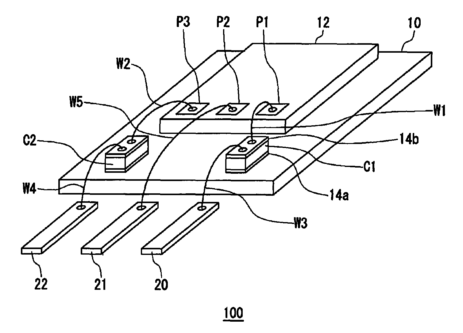
[0038]FIG. 1 is a perspective view of a semiconductor device 100 according to a first embodiment of the present invention. The semiconductor device 100 is configured by a lead frame package. The semiconductor device 100 includes a base substrate 10, a semiconductor substrate 12, shunt capacitors C1 and C2, internal bonding wires W1 and W2, external bonding wires W3 and W4, a direct bonding wire W5, and lead electrodes (merely called as lead below) 20 to 22. In fact, the semiconductor device 100 is sealed with a molding resin; however, in order to clarify an internal structure, the molding resin is not shown.

[0039]At least the surface of the base substrate 10 is formed of a conductive material. The “surface” in this case represents only one side of the base substrate 10, or both sides thereof. The base substrate 10 is a member which corresponds to an island of a lead frame. In the present embodiment, the base substrate 10 is formed of metal as a whole as in the island of the lead fra...

second embodiment

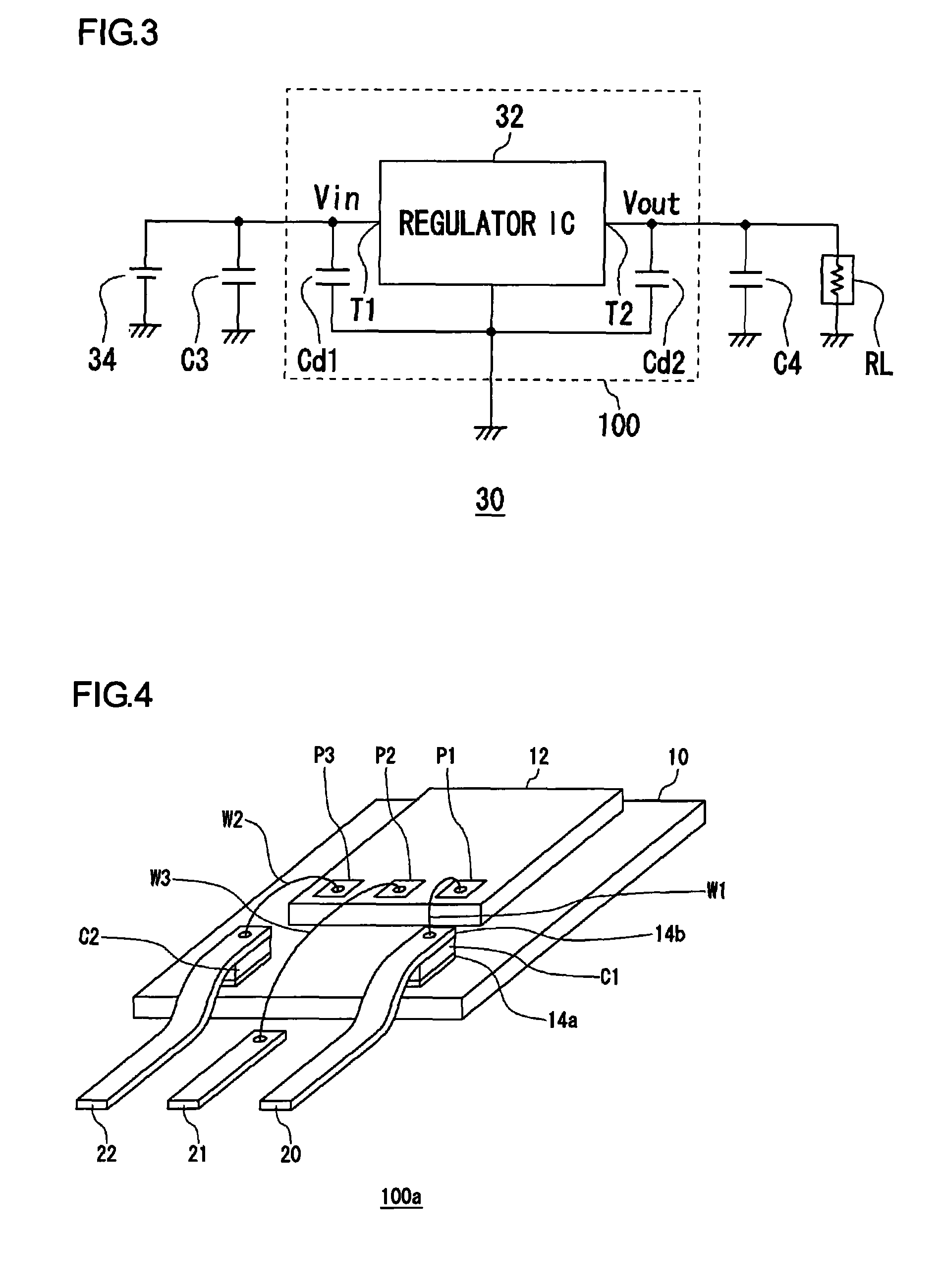
[0056]FIG. 4 is a perspective view of a semiconductor device 100a according to a second embodiment. A structure of the semiconductor device 100a according to the second embodiment will be described below covering mainly the different points from the semiconductor device 100 shown in FIG. 1. In a semiconductor device 100a shown in FIG. 4, a connection configuration of a pad P1, a shunt capacitor C1, a lead 20, and an internal bonding wire W1 is different from that of the semiconductor device 100 shown in FIG. 1.

[0057]In the semiconductor device 100a shown in FIG. 4, a lead 20 is formed in a folded shape, extended so as to cover over the second electrode 14b of the shunt capacitor C1, and directly connected to the second electrode 14b of a shunt capacitor C1 without via a bonding wire. Furthermore, the pad P1 of a semiconductor substrate 12 is connected to the lead 20 via the internal bonding wire W1. In addition, a shunt capacitor C2 is also connected in the same way as the shunt cap...

third embodiment

[0065]FIG. 5 is a perspective view of a semiconductor device 100 according to a third preferred embodiment of the present invention. The semiconductor device 100 is configured by a lead frame package. The semiconductor device 100 includes a base substrate 10, a semiconductor substrate 12, lead electrodes (merely referred to as lead below) 21 to 23, an island 18, and bonding wires W1 to W3. The bonding wire is a gold wire, for example. In fact, the semiconductor device 100 is sealed with a molding resin; however, in order to clarify the internal structure, the molding resin is not shown.

[0066]The semiconductor substrate 12 is a semiconductor chip in which an integrated circuit is formed. The semiconductor substrate 12 is mounted on a first electrode 14 of the base substrate 10, and a ground potential is supplied from the first electrode 14 of the base substrate 10. In addition, a plurality of pads P1 to P3 which are provided for external connection are provided on the semiconductor s...


PUM


Abstract

A semiconductor device has a package structure provided with leads that are external connection terminals. A base substance is an island, and at least the surface thereof is formed of a conductive material. A semiconductor substrate is mounted on the surface of the base substance, and a ground potential is supplied from the surface of the base substance. A shunt capacitor is provided with an electrode pair of a first electrode and a second electrode formed in parallel, and mounted with the first electrode being electrically connected to the surface of the base substance. An internal bonding wire connects a pad provided on the semiconductor substrate for external connection, to the second electrode of the shunt capacitor. The lead is the external connection terminal of the semiconductor device. An external bonding wire connects the lead to the second electrode of the shunt capacitor.

Description

BACKGROUND OF THE INVENTION[0001]1. Field of the Invention[0002]The present invention relates to a semiconductor device having a configuration in which a semiconductor element and a chip component are mounted on inner leads, and the resultant structure is sealed with a molding resin.[0003]2. Description of the Related Art[0004]A semiconductor device having a quad flat package (referred to as QFP) structure or the like includes a semiconductor chip on which an integrated circuit is formed and a conductor called as a lead frame. The semiconductor chip is mounted on an island of the lead frame, and pads provided on the semiconductor chip are connected to leads via bonding wires; and then, the resultant structure is sealed with a molding resin. After that, a semiconductor package is separated from the lead frame.[0005][Patent Document 1] Japanese Patent Application Laid-open No. 2002-231875.[0006]The case where a power supply circuit such as a linear regulator (three terminal regulator)...

Claims


Application Information

Patent Timeline
Patent Type & Authority Patents(United States)
IPC IPC(8): H01L23/48
CPCH01L23/49531H01L24/49H01L23/49589H01L2924/014H01L2224/45144H01L2224/48091H01L2224/48195H01L2224/48247H01L2224/48464H01L2224/4911H01L2924/01005H01L2924/01014H01L2924/01015H01L2924/01022H01L2924/01079H01L2924/01082H01L2924/14H01L2924/19041H01L2924/30107H01L2924/01033H01L2924/01006H01L24/48H01L2924/00014H01L2924/181H01L24/45H01L2924/00H01L2224/05599
Inventor HIRAGA, NORIAKI
Owner ROHM CO LTD
Why Eureka
Try Eureka