Semiconductor laser apparatus

a laser and semiconductor technology, applied in the direction of solid-state devices, dc-dc conversion, lasers, etc., can solve the problems of increasing the manufacturing cost, reducing thermal reliability, etc., and achieve the effect of suppressing the occurrence of stress, reducing the area of the semiconductor laser chip, and reducing the amount of heat loss

Active Publication Date: 2011-05-24
PANNOVA SEMIC
View PDF8 Cites 1 Cited by
  • Summary
  • Abstract
  • Description
  • Claims
  • Application Information

AI Technical Summary

Benefits of technology

[0007]The present invention has been devised in view of the foregoing problems. An object of the present invention is to provide a semiconductor laser apparatus which can suppress the occurrence of a stress caused by a structure in a semiconductor laser chip having a long laser cavity length without increasing the area of the semiconductor laser chip or interfering with heat radiation, so that a crack and a fracture can be suppressed on the semiconductor laser chip.
[0009]In the long and thin semiconductor laser chip, the recessed marks are limited to the surface of the electrode within the predetermined distance from each of the front and rear end faces of the resonator direction, so that further stress concentration can be avoided at the center of the resonator direction where a stress has been concentrated. Thus it is possible to suppress a crack and a fracture which are caused by a temperature change and a mechanical stress on the semiconductor laser chip.

Problems solved by technology

However, as the laser cavity length of the semiconductor laser chip increases, a stress caused by assembling or the structure is applied in a direction that pulls the semiconductor laser chip.
However, this method increases the area of the semiconductor laser chip and the manufacturing cost.
However, this method interferes with heat radiation and thus reduces thermal reliability particularly in a high-power semiconductor laser chip.

Method used


Image

  • Semiconductor laser apparatus
  • Semiconductor laser apparatus
  • Semiconductor laser apparatus

Examples


Embodiment Construction

)

[0024]An embodiment of the present invention will be described below with reference to the accompanying drawings.

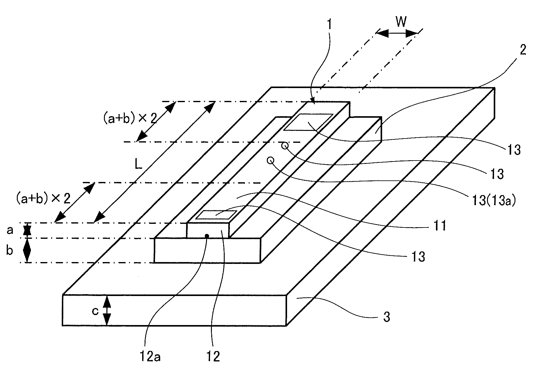
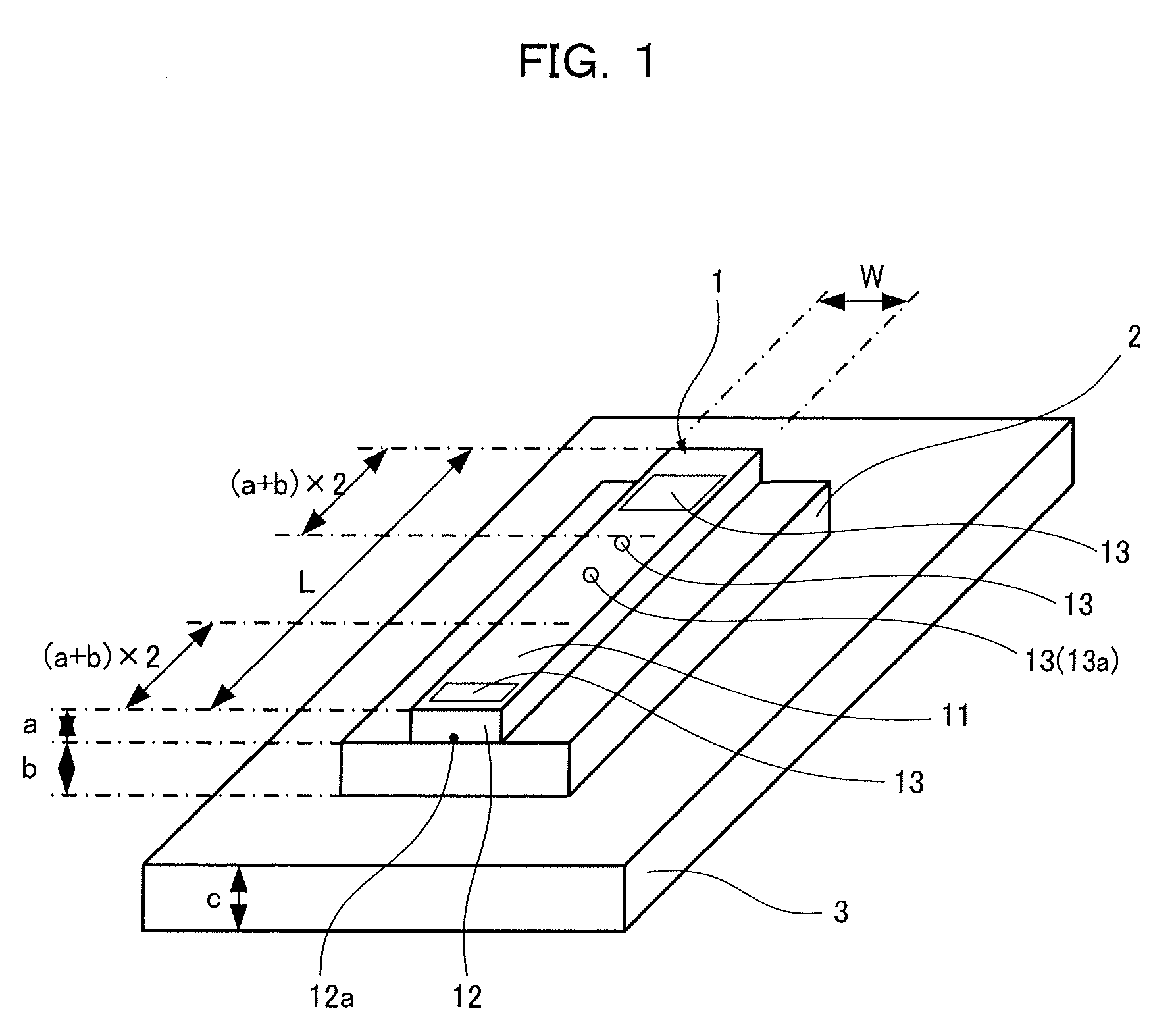
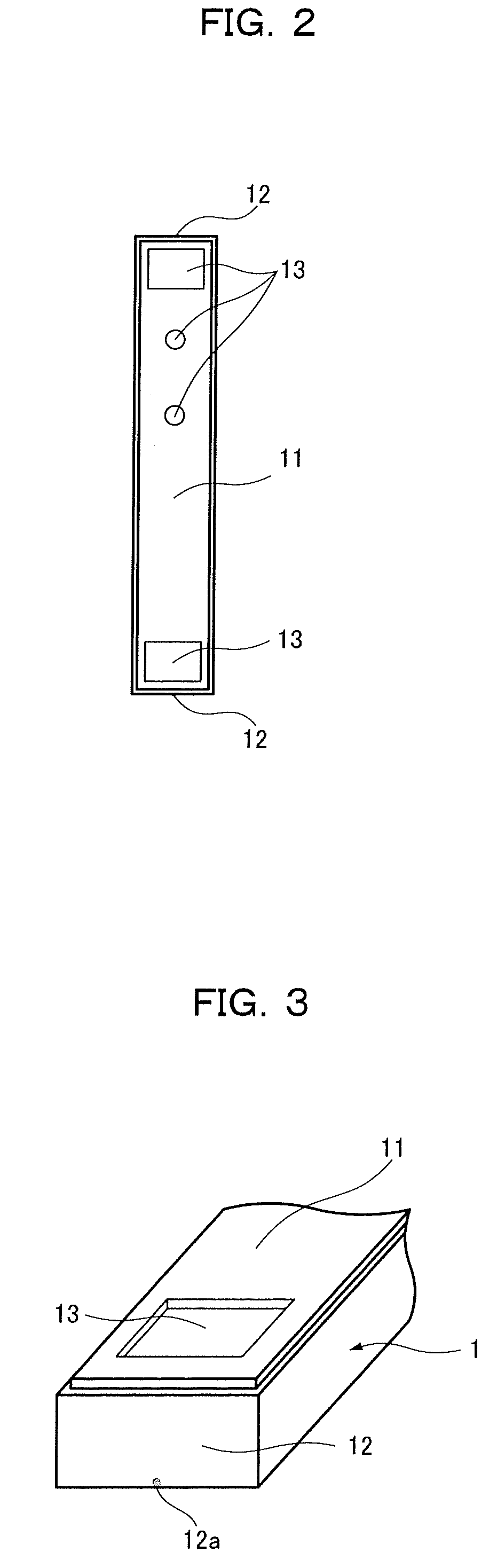
[0025]As shown in FIGS. 1 to 3, a semiconductor laser apparatus includes a semiconductor laser chip 1 for passing current in the thickness direction and a heat sink 3 on which the semiconductor laser chip 1 is bonded via a submount 2. The semiconductor laser chip 1 has electrodes 11 formed on both surfaces (the electrode on the undersurface is not shown) and has an emission region 12a on one end face 12. A length L in the resonator direction is larger than a length W in a direction orthogonal to the resonator direction. On the top surface of the semiconductor laser chip 1, recessed marks 13 for recognition and positioning are disposed within a predetermined distance from each of the front and rear end faces of the resonator direction.

[0026]The semiconductor laser chip 1 is made up of a semiconductor substrate mainly composed of gallium arsenide. The submount 2 is a subst...


PUM


Abstract

A semiconductor laser apparatus of the present invention includes: a semiconductor laser chip 1 having an electrode 11 formed on a surface of the semiconductor laser chip 1; a heat sink 3 for the semiconductor laser chip 1; a submount 2 disposed between the semiconductor laser chip 1 and the heat sink 3 and bonded to the semiconductor laser chip 1 and the heat sink 3; and recessed marks 13 formed on the surface of the semiconductor laser chip 1 by partially removing the electrode 11, wherein the semiconductor laser chip 1 is longer in the resonator direction than in a direction orthogonal to the resonator direction, and the recessed marks 13 are disposed within a predetermined distance from each of the front and rear end faces of the semiconductor laser chip.

Description

FIELD OF THE INVENTION[0001]The present invention relates to a semiconductor laser apparatus used for writing, erasing, and reading information on an optical disk.BACKGROUND OF THE INVENTION[0002]In recent years, higher power laser beams have been demanded of semiconductor laser apparatuses used as light sources in optical disk drives to write, erase, and read information on optical disks. This is because high power laser beams can improve writing speeds on optical disks. For this reason, in a semiconductor laser chip, an optical gain region has been expanded by increasing a length (laser cavity length) in an outgoing direction and a radiating area has been also expanded, so that a high optical output has been stably obtained. However, as the laser cavity length of the semiconductor laser chip increases, a stress caused by assembling or the structure is applied in a direction that pulls the semiconductor laser chip.[0003]FIG. 11 shows a semiconductor laser apparatus of the prior art...

Claims


Application Information

Patent Timeline
Patent Type & Authority Patents(United States)
IPC IPC(8): H01S3/00H01S3/04
CPCH02M3/33523H02M1/36H01L2924/3511
Inventor YOSHIKAWA, NORIYUKI
Owner PANNOVA SEMIC
Why Eureka
Try Eureka