

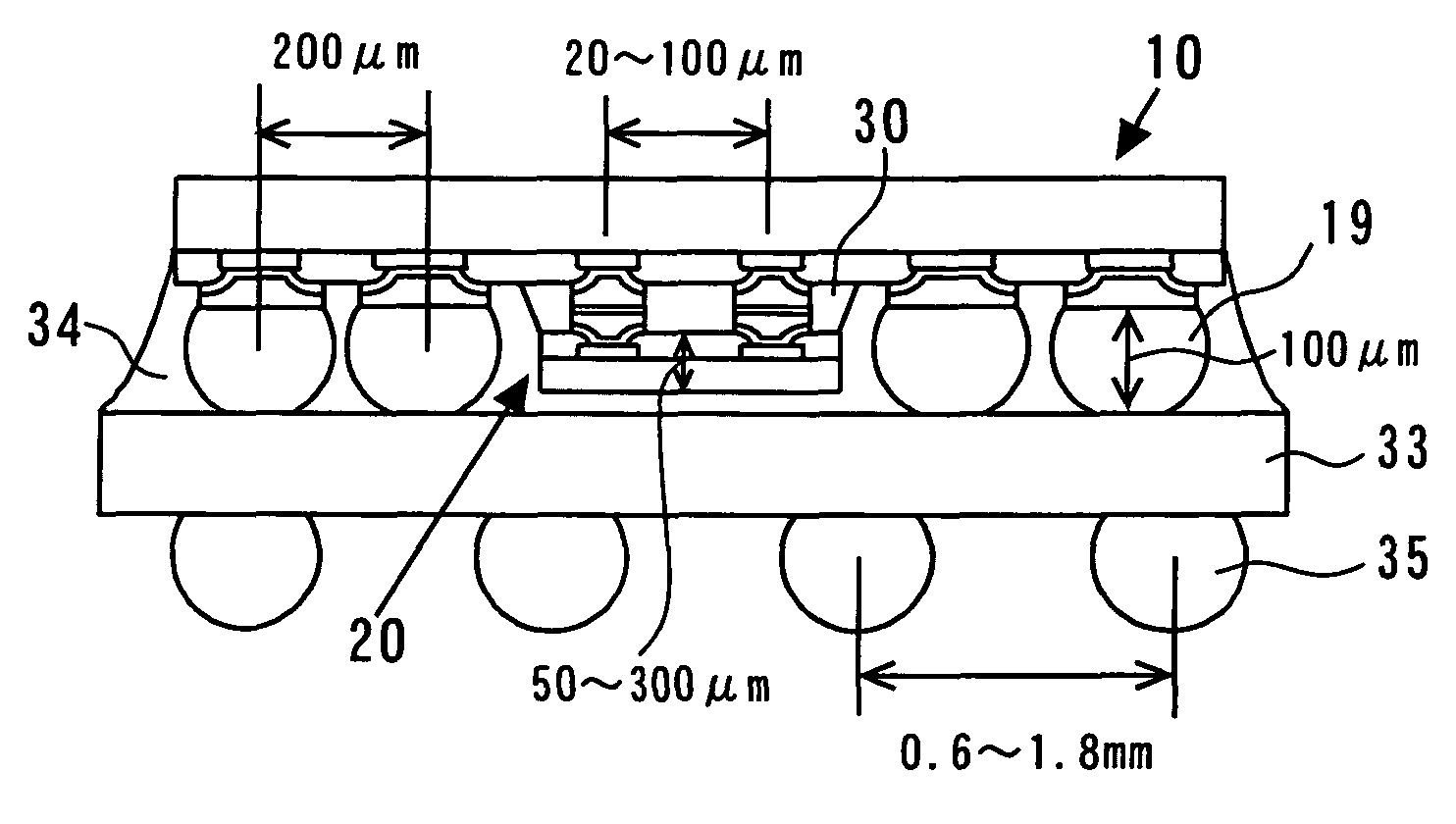
Method of manufacturing semiconductor device
a semiconductor and manufacturing method technology, applied in the direction of semiconductor devices, basic electric elements, electrical appliances, etc., can solve the problems of failure of connection between the mother chip and the daughter chip, the thin oxide film on the surface of the solder film cannot be broken, etc., to prevent the failure of connection
- Summary
- Abstract
- Description
- Claims
- Application Information
AI Technical Summary
Benefits of technology
Problems solved by technology
Method used
Image

Examples
first embodiment
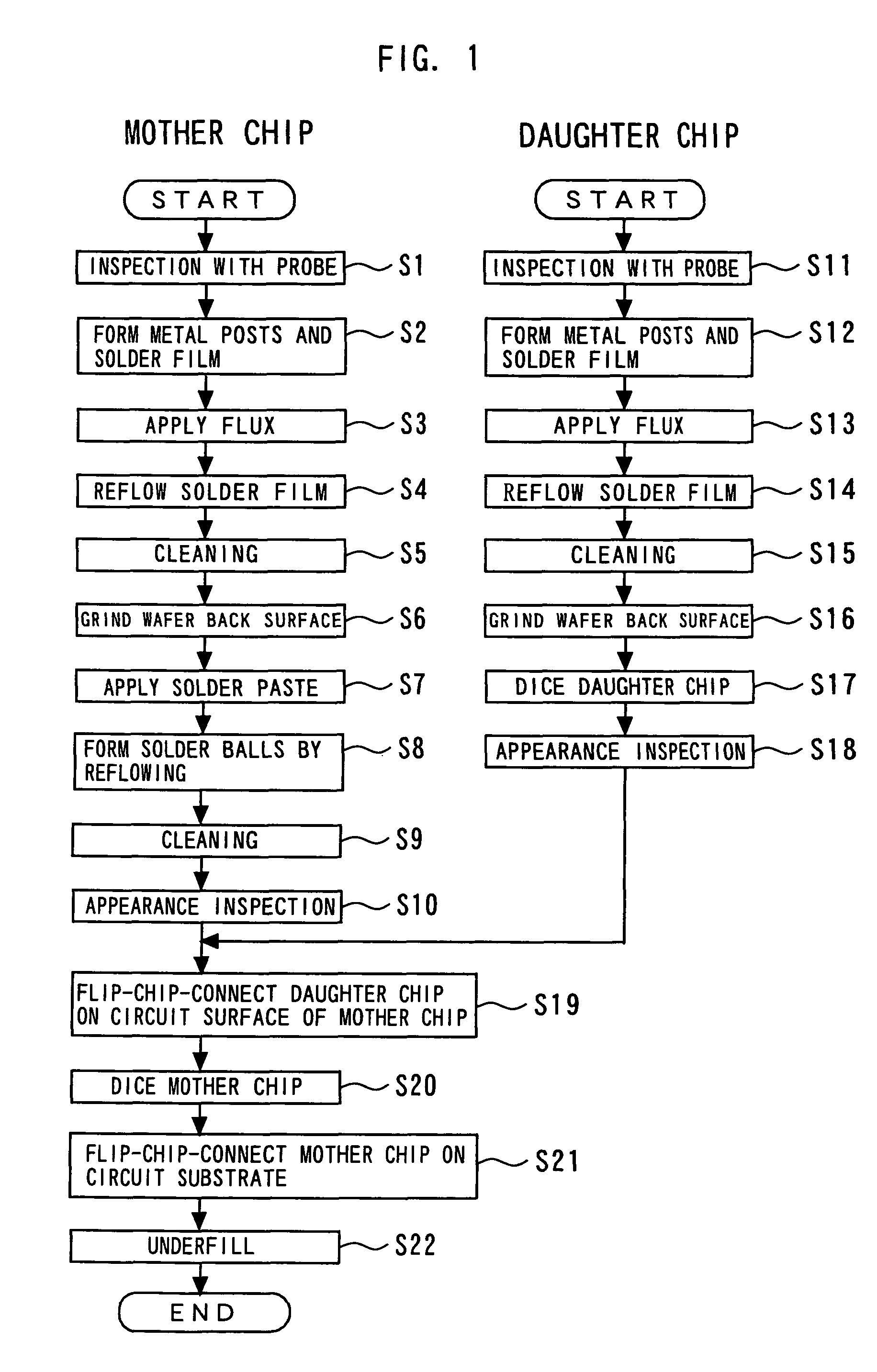
A method of manufacturing a semiconductor device according to a first embodiment of the present invention will be described with reference to the flowchart of FIG. 1 and other figures.
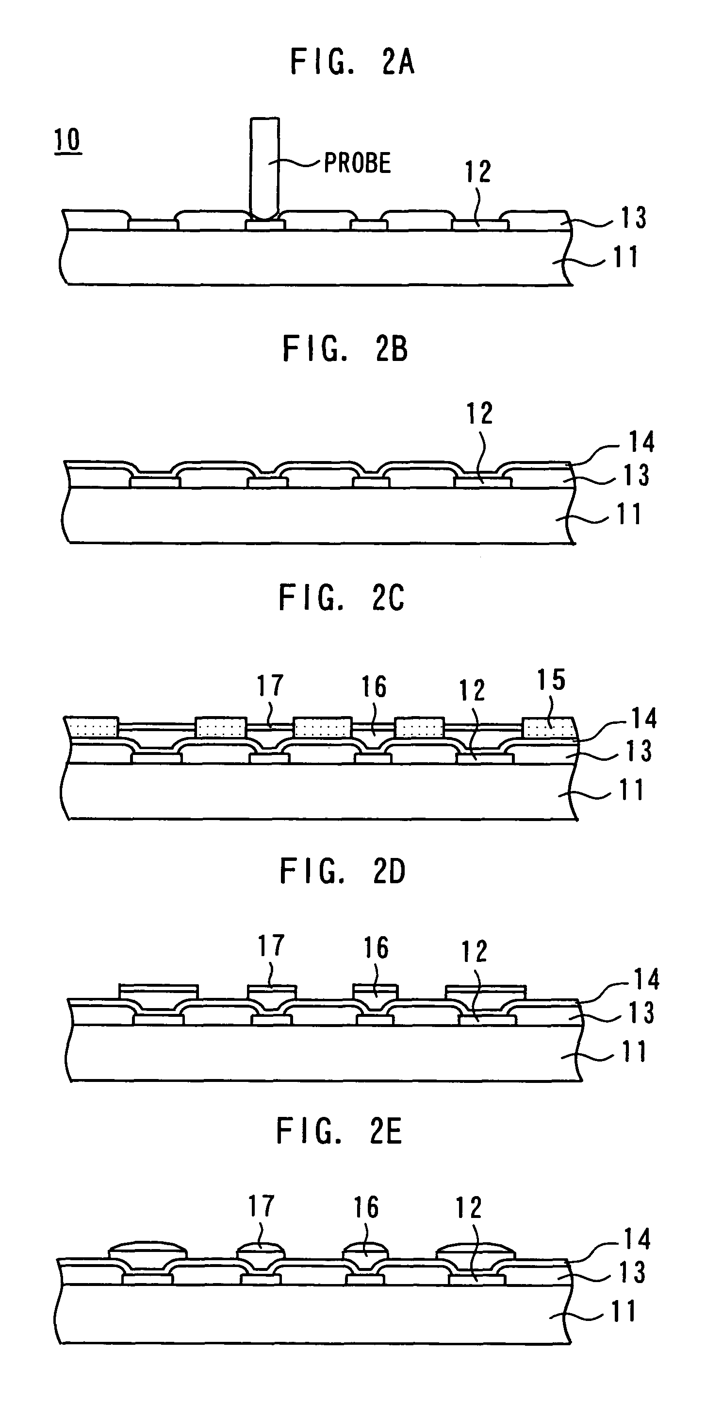
A process of forming a mother chip 10 will first be described. As shown in FIG. 2A, Al electrodes 12 are first formed on a substrate 11 (circuit surface) and other regions are covered, for example, with a surface protective film 13 formed of silicon nitride film and polyimide film. An inspection is made by applying a probe to the Al electrodes 12 (step S1). This inspection is made on each of a plurality of mother chips 10 formed on the wafer, and a wafer map indicating the nondefective / defective state of each mother chip 10 on the wafer is made.
Subsequently, as shown in FIG. 2B, barrier metal 14 in multilayer form comprising Ti, Cu, Ni, Cr and W for example is formed on the entire surface by a sputtering technique or a plating technique for example. As shown in FIG. 2C, a resist 15 having openings corr...
second embodiment
In a second embodiment of the present invention, reflowing for forming solder balls in a nitrogen atmosphere as in the first embodiment is not performed but the oxide film formed in the surface of the solder film is removed by hydrogen plasma after the formation of solder balls. That is, after the solder ball 19 ref lowing step, the oxide film formed in the surface of the solder film 17 is removed or the oxide film thickness is reduced to a value small enough to avoid the problem (several nanometers or less). Joining in the subsequent chip-on-chip connection step can be improved in this way. As a means for removing or reducing the oxide film as described above, exposure of the oxide film to a hydrogen plasma atmosphere, i.e., a reducing plasma, is conceivable. By the reducing action of hydrogen radicals generated in the hydrogen plasma, the oxide film can be effectively removed or reduced. The other steps are the same as those in the first embodiment. The same effect as that in the ...
third embodiment
In a third embodiment of the present invention, reflowing for forming solder balls in a nitrogen atmosphere as in the first embodiment is not performed, but, after the solder ball 19 reflow step, a reducing flux is applied to the entire surface of the mother chip 10 wafer and a heat treatment is performed thereon. The oxide film can be removed or reduced by the reducing action of the flux. That is, after the solder ball 19 ref lowing step, the oxide film formed in the surface of the solder film 17 is removed or the oxide film thickness is reduced to a value small enough to avoid the problem (several nanometers or less). Joining in the subsequent chip-on-chip connection step can be improved in this way. The other steps are the same as those in the first embodiment. The same effect as that in the first embodiment is achieved in this way.
PUM
| Property | Measurement | Unit |
|---|---|---|
| thickness | aaaaa | aaaaa |
| thickness | aaaaa | aaaaa |
| thickness | aaaaa | aaaaa |
Abstract
Description
Claims
Application Information