
Semiconductor laser and method of making semiconductor laser

a semiconductor laser and semiconductor technology, applied in semiconductor lasers, laser details, optical resonator shape and construction, etc., can solve the problems of increasing the optical loss of the active layer, complicated preparation process of this semiconductor laser, and complex preparation process, so as to achieve satisfactory temperature characteristics, simplify the preparation process, and satisfy the effect of characteristics

Active Publication Date: 2011-06-07
SUMITOMO ELECTRIC IND LTD
View PDF3 Cites 0 Cited by
  • Summary
  • Abstract
  • Description
  • Claims
  • Application Information

AI Technical Summary

Benefits of technology

The present invention provides a semiconductor laser that does not have a butt joint structure and includes a laser cavity with a simple structure. The laser cavity includes a first optical confinement layer, a second optical confinement layer, and a diffraction grating. The first quantum wires and the buried semiconductor regions have a refractive index different from the refractive index of the second quantum wires, which helps decrease optical coupling loss. The reflectivity of the first distributed Bragg reflector is higher than the reflectivity of the second distributed Bragg reflector, and the bandwidth of the stop-band of the first distributed Bragg reflector is larger than the bandwidth of the stop-band of the second distributed Bragg reflector, which results in a single longitudinal mode output. The width of each quantum wire in the direction of the predetermined axis may be larger than the width of each other quantum wire.

Problems solved by technology

Thus, the preparation process is complicated.
Accordingly, the preparation process of this semiconductor laser is complicated.
Furthermore, since the impurity is added to an active layer, the optical loss of the active layer increases.

Method used


Image

  • Semiconductor laser and method of making semiconductor laser
  • Semiconductor laser and method of making semiconductor laser
  • Semiconductor laser and method of making semiconductor laser

Examples


Embodiment Construction

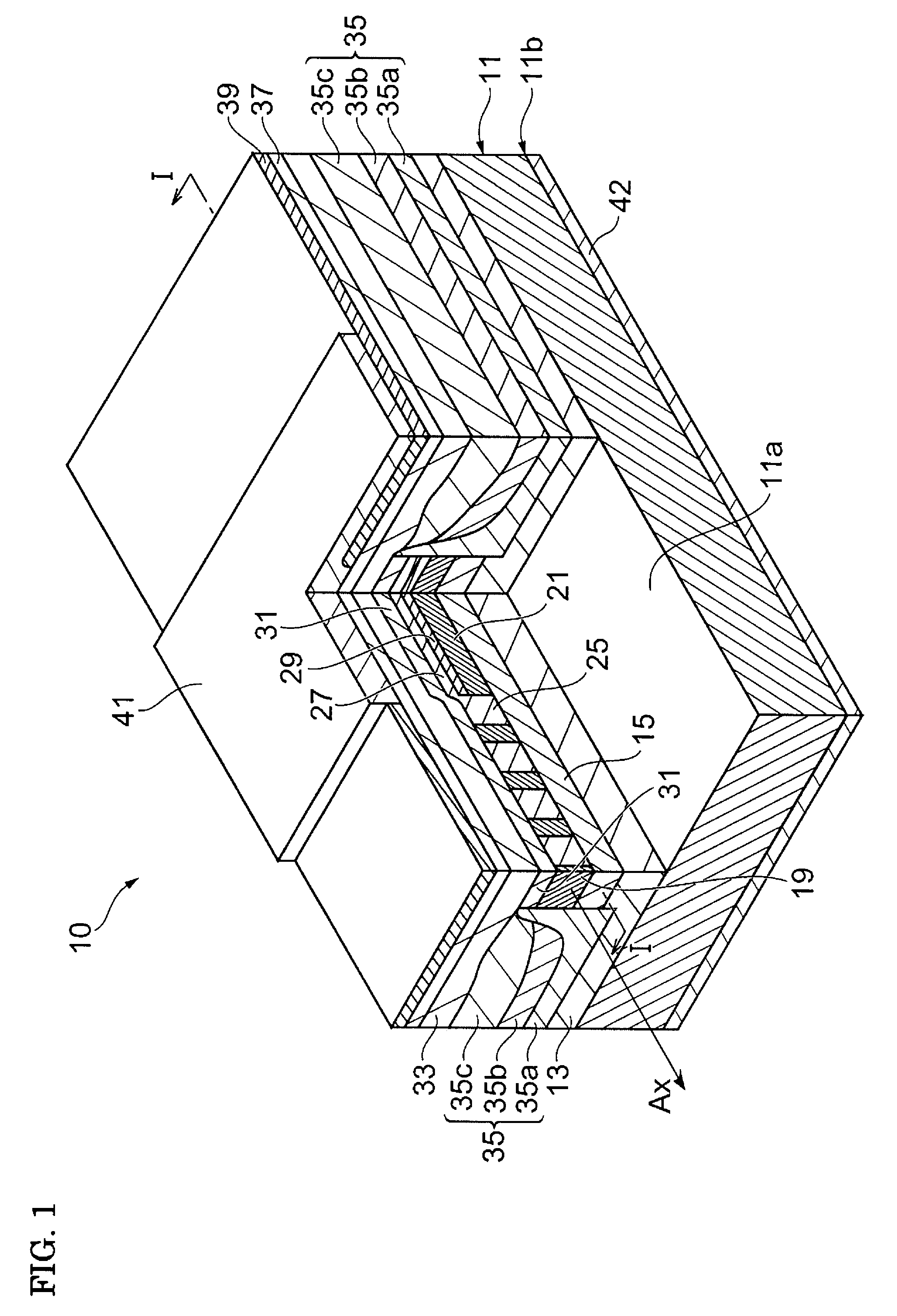
[0040]Findings of the present invention can be easily understood by considering the detailed description below with reference to the attached drawings shown as exemplifications. Next, semiconductor lasers and a method of making a semiconductor laser according to embodiments of the present invention will now be described with reference to the attached drawings. The same components are assigned the same reference numerals for each possible case.

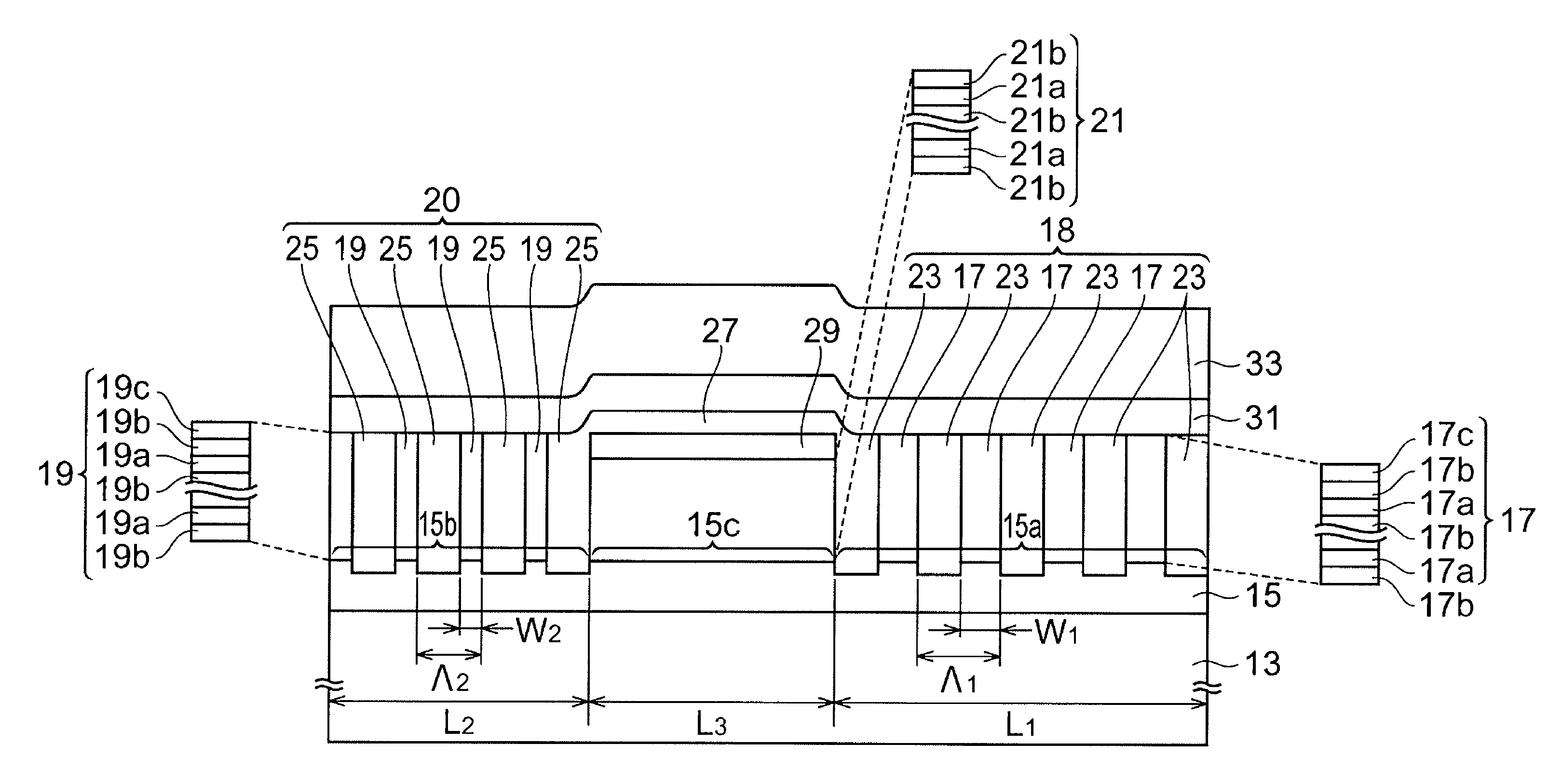
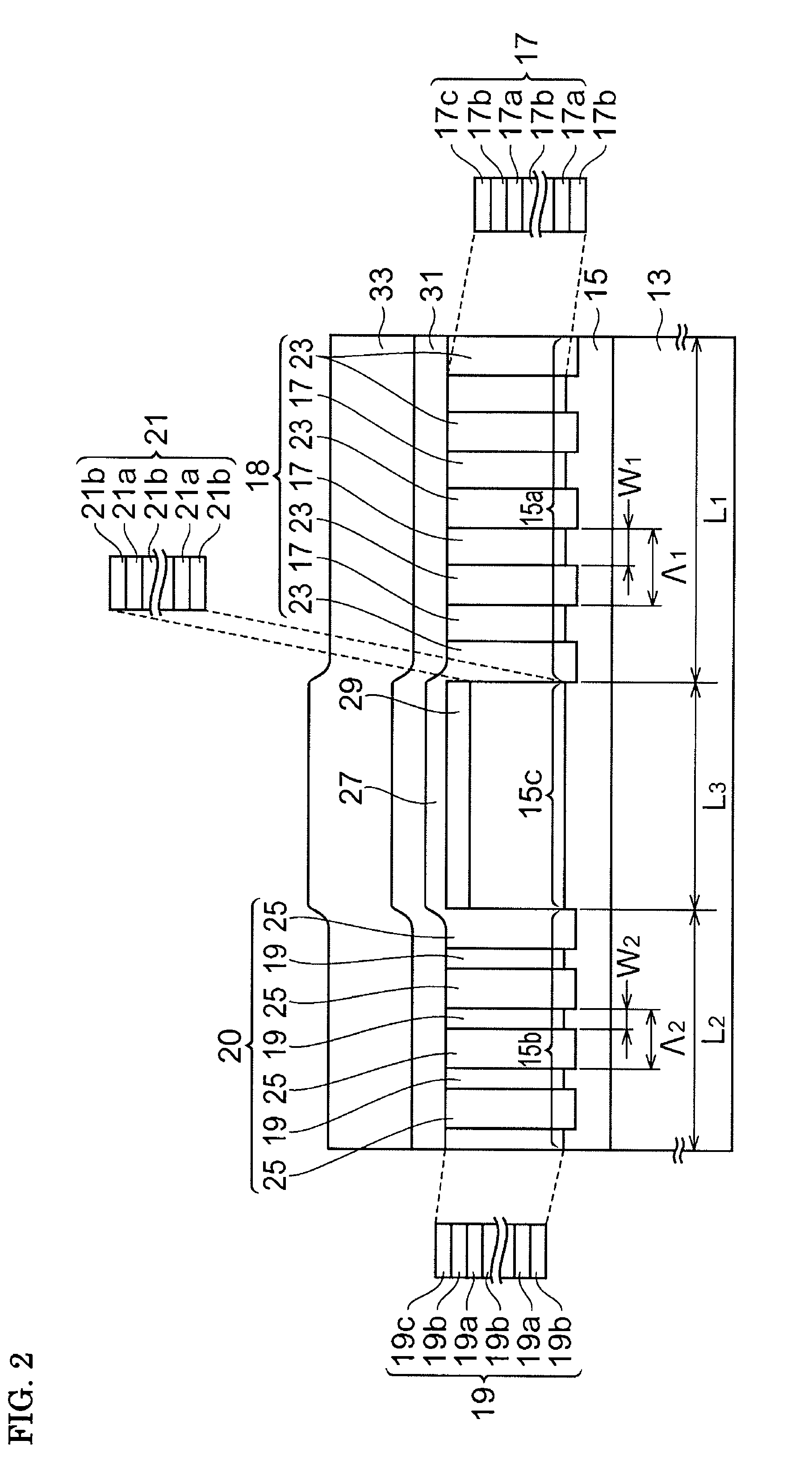
[0041]FIG. 1 is a perspective view showing the structure of a semiconductor laser according to a first embodiment of the present invention. FIG. 2 is a cross-sectional view taken along line I-I of FIG. 1. A semiconductor laser 10 includes a first cladding layer 13, a first optical confinement layer 15, a first distributed Bragg reflector 18, a second distributed Bragg reflector 20, an active layer 21, a second optical confinement layer 31, and a second cladding layer 33. The first cladding layer 13 is provided on a main surface 11a of a semicon...


PUM


Abstract

A semiconductor laser includes a first optical confinement layer, a plurality of first quantum wires and buried semiconductor regions disposed on a first area, a plurality of second quantum wires and buried semiconductor regions disposed on a second area, an active layer disposed on a third area, and a second optical confinement layer. The plurality of first quantum wires and the buried semiconductor regions constitute a first distributed Bragg reflector, and the plurality of second quantum wires and the buried semiconductor regions constitute a second distributed Bragg reflector. The third area is disposed between the first area and the second area. The buried semiconductor regions have a refractive index different from the average refractive index of the first quantum wires and the average refractive index of the second quantum wires. These distributed Bragg reflectors form a DBR laser having a cavity length defined by the length of the active layer.

Description

BACKGROUND OF THE INVENTION[0001]1. Field of the Invention[0002]The present invention relates to a semiconductor laser and a method of making a semiconductor laser.[0003]2. Description of the Related Art[0004]A distributed Bragg reflector laser (DBR laser) includes an active layer region and distributed Bragg reflector mirrors (DBR mirrors) provided at both sides of the active layer region. In general, in order to reduce the loss of the DBR mirrors, the energy gap (Eg) of a material constituting the DBR mirrors is set so as to be larger than the Eg of the active layer. Reference 1 (K. Shinoda et al.: The 19th International Conference on Indium Phosphide and Related materials (IPRM 2007), TuB2-3, 39, 15 May 2007) describes a short-cavity DBR laser. This DBR laser includes an active layer region having a multi-quantum well structure composed of InGaAlAs and DBR mirrors in which a diffraction grating is formed on an optical waveguide layer composed of InGaAsP. A butt joint structure is...

Claims


Application Information

Patent Timeline
Patent Type & Authority Patents(United States)
IPC IPC(8): H01S5/00
CPCB82Y20/00H01S5/125H01S5/0654H01S5/1039H01S5/1215H01S5/1231H01S5/34306H01S5/2009H01S5/305H01S5/3054H01S5/3211H01S5/341
Inventor YAGI, HIDEKI
Owner SUMITOMO ELECTRIC IND LTD
Learn More