Pulse generation circuit and UWB communication device

a technology of pulse generation circuit and communication device, which is applied in the direction of pulse manipulation, pulse technique, instruments, etc., can solve the problems of difficult to generate a correct pulse, band limitation is necessary to use pulses, and takes a long time, etc., to achieve stable, reliable and sensitive pulses, and low price. , the effect of high availability

Inactive Publication Date: 2011-06-14
138 EAST LCD ADVANCEMENTS LTD
View PDF8 Cites 0 Cited by
  • Summary
  • Abstract
  • Description
  • Claims
  • Application Information

AI Technical Summary

Benefits of technology

[0044]In the UWB communication device of the application example 8, since a very thin and accurate pulse specific to UWB can easily be generated by the pulse generation circuits according to the application examples 1 through 7, by using these circuits as the template pulse generation circuit of the modulation circuit or the demodulation circuit, it becomes possible to adopt such a stable circuit mode, thus it becomes possible to compose a stable, reliable, and sensitive device at a low price. In particular, the pulse generation circuit according to the application examples of the invention is capable of generating an accurate pulse with a frequency as high as the performance limit of the component, and has high availability.
[0045]The pulse generation circuit as the embodiment of the invention can be formed of a CMOS integrated circuit or the like, and is capable of generating a pulse having an accurate waveform with a simple circuit even in the case with the pulse as thin as the operational transition duration of the component. Further, since the circuit can be formed of a logic circuit using a CMOS integrated circuit, it is possible to form a configuration capable of easily operating at the maximum speed of the CMOS circuit without increasing the operating power, thus a high-frequency wide-band pulse, which can be used for the UWB communication, can easily be generated.

Problems solved by technology

Although the transistors 1127 and 1128 also pull back the potential to V0, since these transistors have high on-resistances, it takes long time before the potential reaches V0, which makes it difficult to generate a correct pulse.
However, as is well known, and as shown in FIGS. 17A through 17G, the spectrum characteristics of the pulses generated by the circuit of the related art described above are the sinc function having a very broad side lobe, and therefore, some sort of band limitation is necessary to use the pulses generated by the circuit for communication.
However, as the filter, a bandpass filter with a preferable skirt characteristic in an ultra wide band and at an ultra high frequency close to the performance limit of the elements is required, which is hard to configure.

Method used


Image

  • Pulse generation circuit and UWB communication device
  • Pulse generation circuit and UWB communication device
  • Pulse generation circuit and UWB communication device

Examples


first embodiment

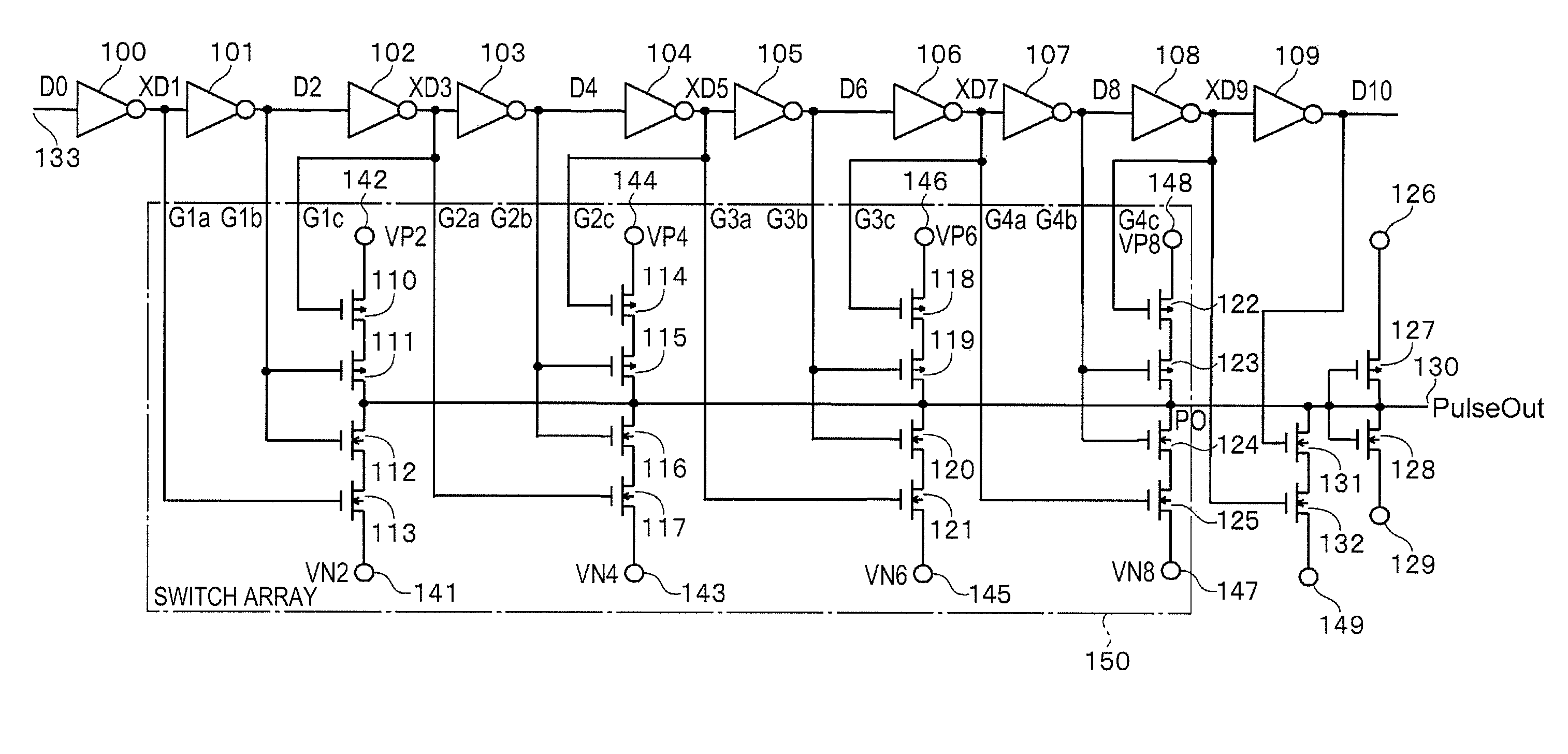
[0082]FIG. 1 shows a first embodiment. FIG. 3 describes the time chart representing the operation thereof.

[0083]The internal configuration of the inverter delay circuits 101 through 109 is substantially the same as the configuration of the inverter delay circuit used in the related art explained with reference to FIG. 16. The amount of delay of each stage of the inverter delay circuits is assumed to be adjusted to PW (125 psec in the case of the present embodiment of the invention). In the case in which the amount of delay takes this value, the target pulse described above, namely the pulse with the carrier frequency f0=4 GHz (the carrier pulse width PW=125 psec) can be generated. Since the inverter delay circuits 100 through 109 delay the start signal D0 while inverting the start signal D0, the outputs thereof are represented as XD1, D2, XD3, . . . , D10 with the symbol X for representing the inverted logic of the signal attached to the front of the name of each of the odd numbered...

second embodiment

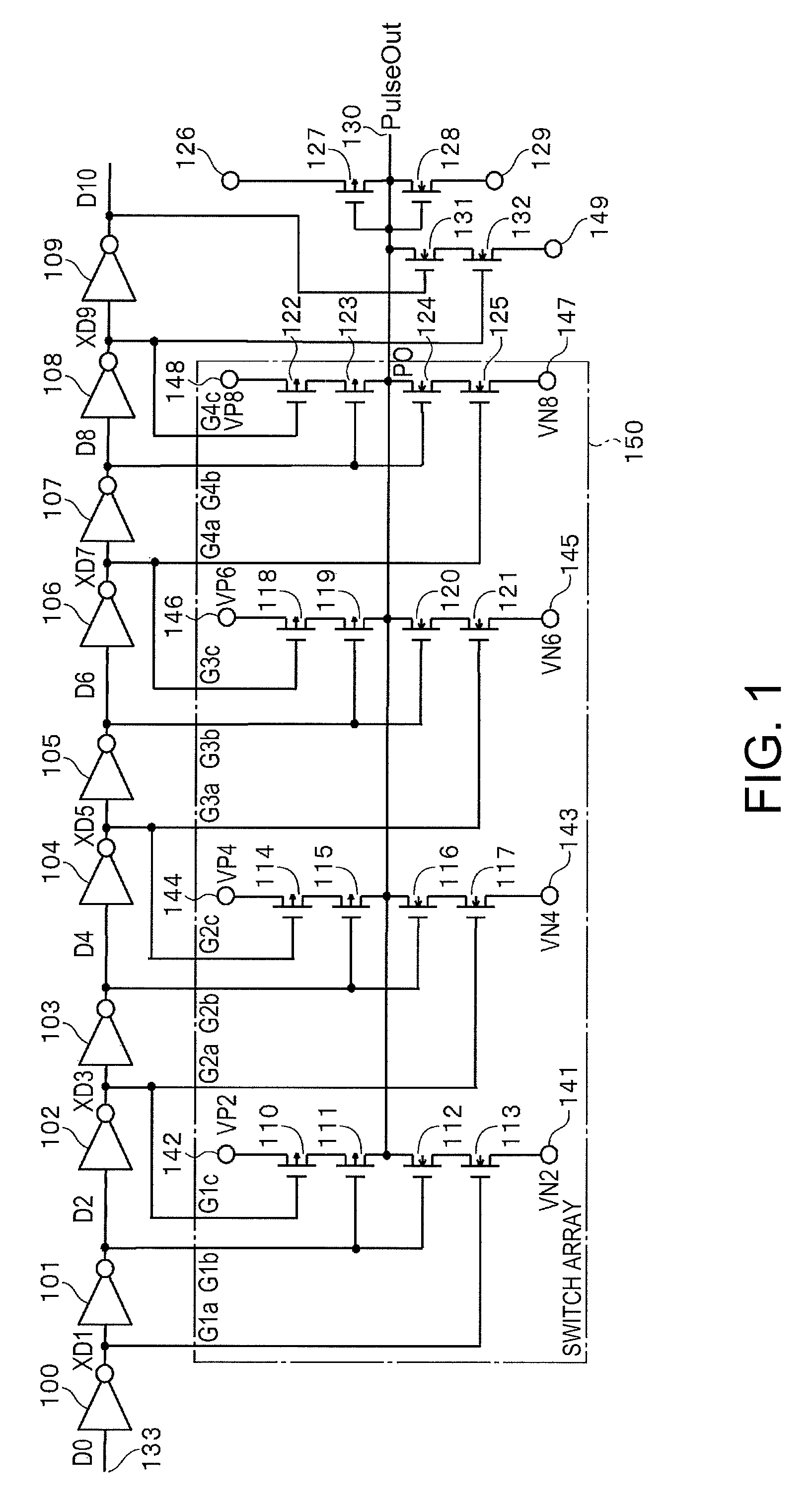
[0095]FIG. 2 shows a second embodiment of the invention. FIG. 3 used commonly to the first embodiment describes the time chart representing the operation thereof. The same elements as those explained in the first embodiment will be denoted in FIG. 2 with the same reference numerals as in FIG. 1, and the explanations therefore will be omitted.

[0096]In the present embodiment, the terminals 142, 144, 146, and 148 provided with VPi connected thereto in the first embodiment are connected to each other, and provided with an output signal V2 of a band-limitation filter 202 connected thereto. Further, the terminals 141, 143, 145, and 147 provided with VNi connected thereto in the first embodiment are connected to each other, and provided with an output signal V1 of a band-limitation filter 203 connected thereto.

[0097]In the present embodiment, the signals V1, V2 described above are generated as follows. Specifically, a logic circuit 201 generates a pulse signal E and a pulse signal XE with ...

third embodiment

[0100]FIG. 4 shows a circuit diagram of a third embodiment, and FIG. 5 shows a time chart for explaining the operation thereof.

[0101]In the drawing, NOR circuits 403, 404, and 405 are delay circuits. The outputs of the respective NOR circuits are defined as Q1, Q2, and Q3. One of two input terminals of the NOR circuits 403, 404, and 405 are respectively connected to the outputs Q3, Q1, and Q2 of the NOR circuits 405, 403, and 404 to form a ring circuit. Further, the other input terminals 408, 407, and 406 of the NOR circuits 403, 404, and 405 are defined as C1, C2, and C3, respectively. A circuit composed of switching transistors 411 through 422 connects the pulse output terminal Pout 410 to the output V1 of a low-pass filter 409 when (Q1+Q2)*(Q3+Q1)*(Q2+Q3) is false, and connects the pulse output terminal Pout 410 to the output V2 of the low-pass filter 424 when Q3*Q1+Q2*Q3+Q1*Q2 is true.

[0102]The part surrounded by the dotted line 423 in the drawing is identical to the original ci...


PUM


Abstract

A pulse generation circuit for outputting a pulse with a predetermined waveform to an output terminal in response to a start signal includes a circuit adapted to generate a plurality of signals {Di|i denotes an integer in a predetermined range}, which has predetermined amounts of time differences from the start signal, based on the start signal, a plurality of power supplies {Ej|j denotes an integer} adopted to supply electric energy of a predetermined electric quantity, and a switching circuit adapted to sequentially switch the power supplies {Ej} in a predetermined order in accordance with logical function values of at least a part of the signals {Di} to connect the power supplies {Ej} to the output terminal.

Description

BACKGROUND[0001]1. Technical Field[0002]The present invention relates to a pulse generation circuit for generating pulses suitable for Ultra Wide Band (UWB) communication, and a UWB communication device.[0003]2. Related Art[0004]The UWB communication is a communication method for performing high speed large capacity data communication using a very wide frequency band. As the communication method using wide-band signals, there are cited a spread spectrum system and orthogonal frequency division multiplexing (OFDM) in the related art. However, UWB is a further wide-band communication method using pulses with very short period of time, and is also called impulse radio (IR) communication. In the IR systems, modulation and demodulation can be performed only by time-base operations in contrast to the modulation in the related art, and simplification of the circuit and reduction of power consumption are considered to be expected (see the specifications of U.S. Pat. No. 6,421,389, US-2003 / 0...

Claims


Application Information

Patent Timeline
Patent Type & Authority Patents(United States)
IPC IPC(8): H02J1/00H02H3/00H03K3/017H04B1/717H04J13/00H04L27/02
CPCH03K5/133H04B1/7172H04L25/03834H04B1/7174H03K2005/00293Y10T307/724Y10T307/702
Inventor IKEDA, MASAYUKI
Owner 138 EAST LCD ADVANCEMENTS LTD
Why Eureka
Try Eureka