Semiconductor memory device for writing data to multiple cells simultaneously and refresh method thereof

a memory device and memory device technology, applied in static storage, digital storage, instruments, etc., can solve the problems of losing even the previously charged power, instant power disconnection, and destroying the data of a ram, so as to improve the data retention of the cell array

Active Publication Date: 2011-06-14
SK HYNIX INC
View PDF9 Cites 18 Cited by
  • Summary
  • Abstract
  • Description
  • Claims
  • Application Information

AI Technical Summary

Benefits of technology

[0054]An embodiment of the present invention writes data simultaneously in a plurality of cells without increasing the write current, thereby reducing the write time of a memory device using a phase change resistor.
[0065]According to an embodiment of the present invention, a refresh method of a semiconductor memory device comprises: sensing changes in crystallization induced through application of currents through the bit line so as to read / write data in the cell array including a phase change resistor configured to store data corresponding to resistance change; and refreshing data of the cell array with a specific refresh cycle so as to improve data retention of the cell array.

Problems solved by technology

Instant disconnection of the power may destroy the data of a RAM because a memory cell of the DRAM is designed based on small charging electrons for maintaining the charged power.
These charging electrons are analogous to a tiny battery that is not continuously recharged, and which may therefore lose even the previously charged power.
However, the conventional DRAM must frequently perform the refresh operation because it is volatile and has a short refresh cycle.
That is, in the conventional DRAM, charges stored in the capacitor C leak over time.
As a result, the DRAM cyclically performs a refresh operation for reading and writing data (for example, every 64 msec), which causes large power consumption and degradation of operational performance.
As such, the number of cells to which date can be written simultaneously is limited resulting in degraded write performance.
Although the conventional phase change memory device has a nonvolatile characteristic, cell data is subject to increasing degradation over time, thereby limiting data retention time.
When current of the bit line BL corresponding to the logic data “1” and “0” is decreased, the data retention characteristic is degraded, resulting in difficulties in retaining the optimum nonvolatile cell storing characteristic for a long period of time.
However, the MRAM using a MTJ cell requires a large write current for writing data in the cell.
As a result, the number of cells to which data can be written simultaneously is limited resulting in degraded write performance.
However, the ReRAM using the RSD requires a large write current for writing data in cells.
As such, the number of cells to which data can be written simultaneously is limited resulting in degraded write performance.

Method used


Image

  • Semiconductor memory device for writing data to multiple cells simultaneously and refresh method thereof
  • Semiconductor memory device for writing data to multiple cells simultaneously and refresh method thereof
  • Semiconductor memory device for writing data to multiple cells simultaneously and refresh method thereof

Examples


Embodiment Construction

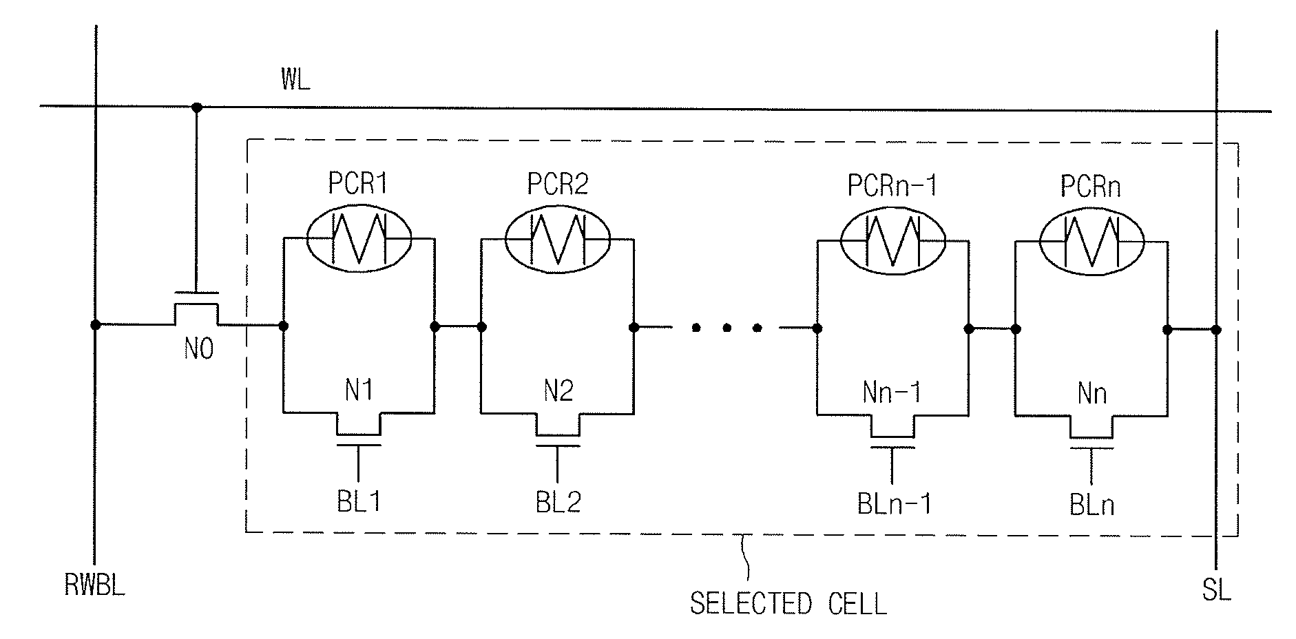
[0108]FIG. 9 is a circuit diagram showing a semiconductor memory device according to an embodiment of the present invention.

[0109]The semiconductor memory device of FIG. 9 comprises a selecting switch SW0, a plurality of cells C1˜Cn, and a plurality of switching elements SW1˜SWn.

[0110]The selecting switch SW0 includes a NMOS transistor. The selecting switch SW0 is connected between a read / write bit line RWBL and a unit cell UC, and the gate of the selecting switch is connected to a word line WL.

[0111]In each unit cell UC a cell C1 is connected in parallel to a switching element SW1. The cell C1 has one electrode connected to the source of the switching element SW1 and the other electrode connected to the drain of the switching element SW1. Gates of the switching elements SW1˜SWn are each connected one by one to a predetermined bit line of a plurality of bit lines BL1˜BLn.

[0112]The cells C1˜Cn are connected between the selecting switch SW0 and the source line SL. That is, the source ...


PUM


Abstract

A semiconductor memory device includes a read / write bit line configured to supply a cell driving voltage. A selecting unit is connected to the read / write bit line and is controlled by a word line. A plurality of cells are connected between the selecting unit and a source line, and the cells are configured to read and write data according to a cell driving voltage. Each switching element of a plurality of switching elements are connected in parallel with a single cell of the plurality of cells, and the plurality of switching elements are controlled selectively by a plurality of bit lines.

Description

CROSS-REFERENCES TO RELATED APPLICATIONS[0001]The present application claims priority to Korean Patent Application Nos. 10-2007-0091732 and 10-2007-0096991 filed on Sep. 10, 2007 and on Sep. 21, 2007 which are incorporated herein by reference in their entirety.BACKGROUND OF THE INVENTION[0002]The present invention relates generally to a semiconductor memory device and a refresh method thereof, and more particularly, to a semiconductor memory device configured to write data simultaneously in a plurality of cells without increasing a write current.[0003]Recently, the demand for semiconductor devices has increased due to the rapid distribution of computers. These semiconductor devices are required to operate at high-speed with high accumulating capacity. As a result, various manufacturing techniques have been developed to improve the integration, response speed, and reliability of the semiconductor devices.[0004]Dynamic Random Access Memory (DRAM), configured to input and output inform...

Claims


Application Information

Patent Timeline
Patent Type & Authority Patents(United States)
IPC IPC(8): G11C11/00
CPCG11C8/06G11C13/0004G11C13/0007G11C13/003G11C13/0033G11C13/004G11C13/0069G11C16/3431G11C8/18G11C2213/76G11C2013/0052G11C2013/0078G11C2013/009G11C2013/0092G11C2213/15G11C2213/31G11C2213/32G11C2213/72G11C2213/75
Inventor KANG, HEE BOKHONG, SUK KYOUNG
Owner SK HYNIX INC
Why Eureka
Try Eureka