Semiconductor device

a technology of semiconductor devices and semiconductors, applied in the direction of semiconductor devices, basic electric elements, electrical equipment, etc., can solve the problems of loss of desired high breakdown voltage characteristics, and achieve the effect of improving the high breakdown voltage performance of semiconductor devices

Active Publication Date: 2011-06-28
SEMICON COMPONENTS IND LLC
View PDF5 Cites 6 Cited by
  • Summary
  • Abstract
  • Description
  • Claims
  • Application Information

AI Technical Summary

Benefits of technology

[0009]The present invention has been made based on these understandings, and a general purpose thereof is to provide a technology for improving the high breakdown voltage performance of a semiconductor device such as DMOS transistors.

Problems solved by technology

And the result will be the loss of desired high breakdown voltage characteristic.

Method used


Image

  • Semiconductor device
  • Semiconductor device
  • Semiconductor device

Examples


first embodiment

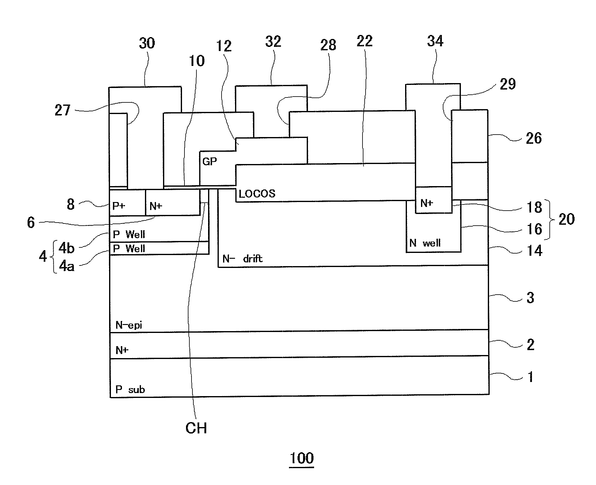
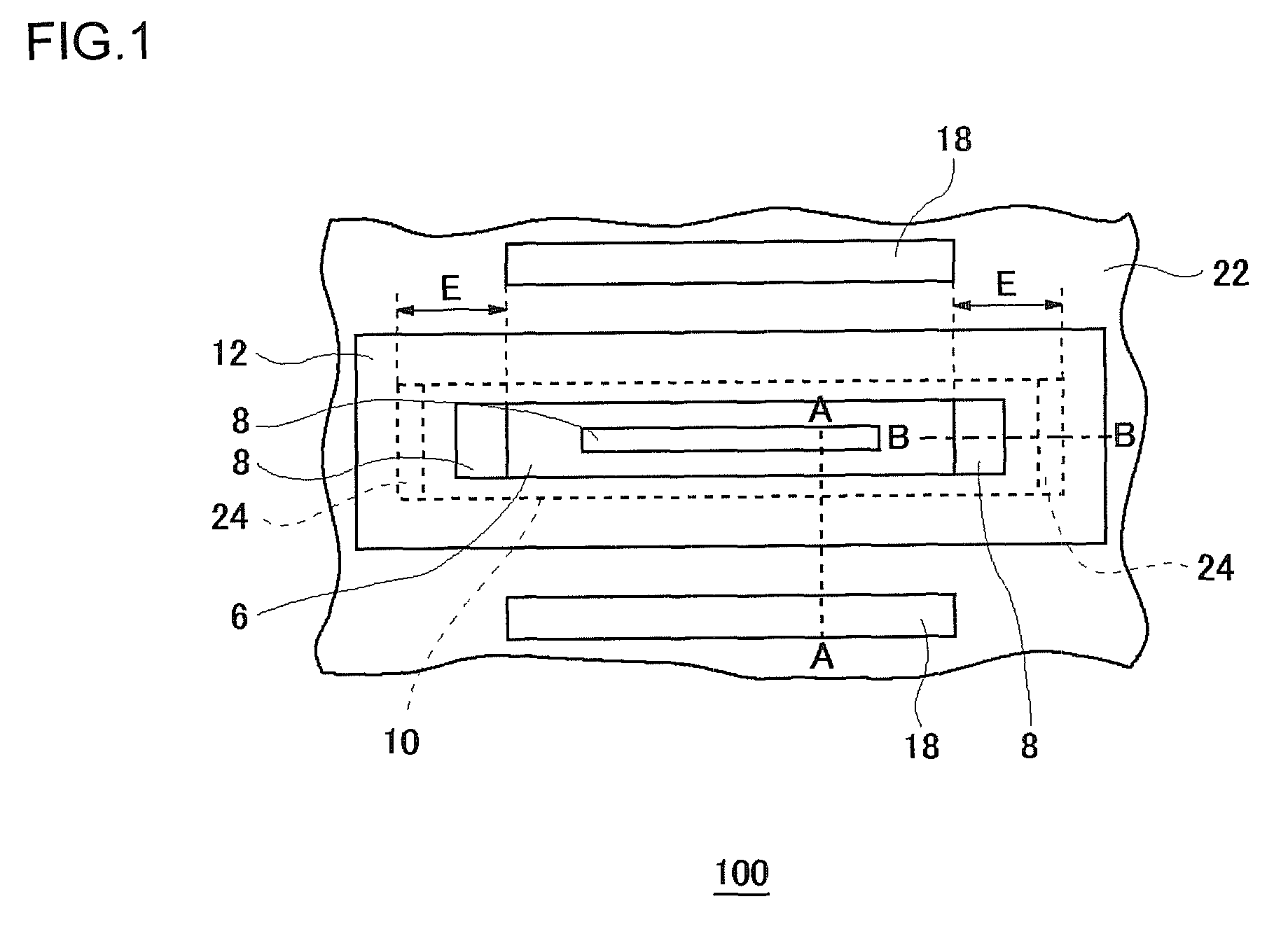
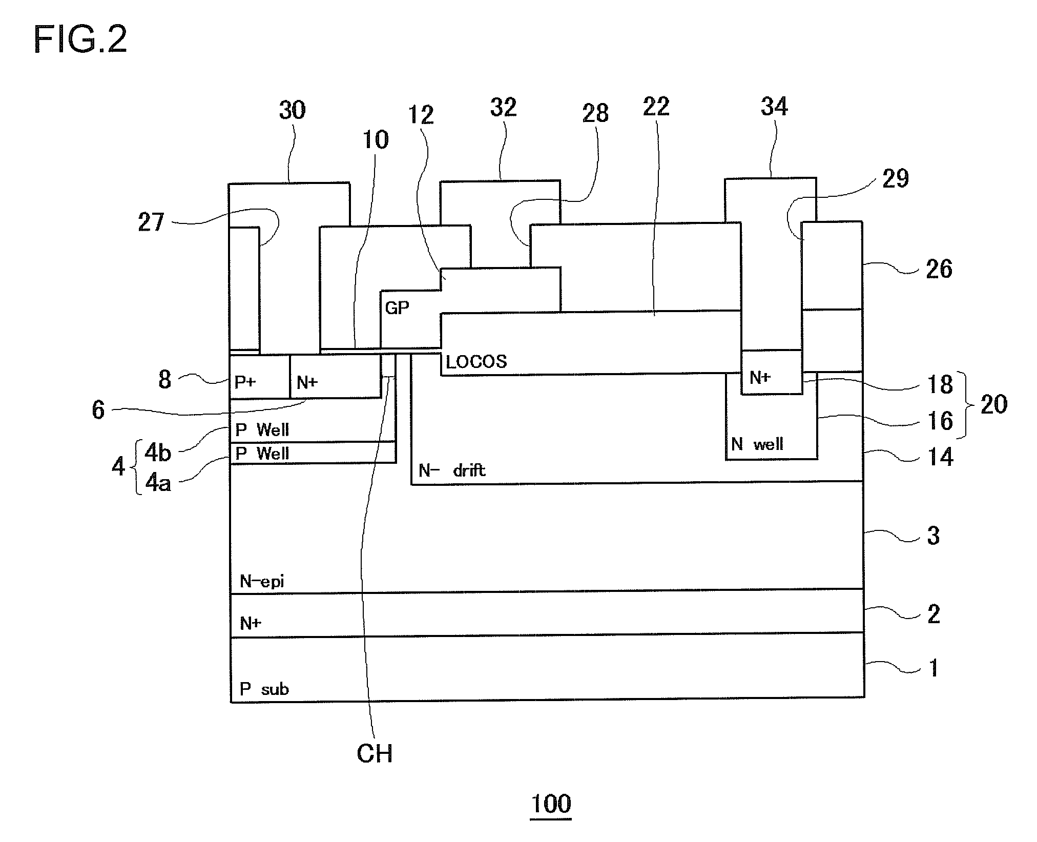
[0043]FIG. 1 is a schematic plan view of a semiconductor device 100 according to a first embodiment of the present invention. FIG. 2 is a cross-sectional view taken along the line A-A of FIG. 1. FIG. 3 is a cross-sectional view taken along the line B-B of FIG. 1. The first embodiment will be described using an N-channel type LDMOS transistor as an example of the semiconductor device 100. Note that in FIG. 1, interlayer insulation films, electrodes, and the like are omitted for ease of explanation.

[0044]As illustrated in FIGS. 1 to 3, the semiconductor device 100 includes a P-type, single-crystal silicon substrate 1, an N+-buried semiconductor layer 2 formed on the silicon substrate 1, and an N−-epitaxial layer 3 (semiconductor layer) formed on the buried semiconductor layer 2. In the first embodiment, only one epitaxial layer 3 is used, but a plurality of epitaxial layers may be stacked. Formed in a surface of the epitaxial layer 3 is a P-type body layer 4 in which a P-type impurity...

second embodiment

[0072]In a second embodiment of the present invention, the region where the thick film portion 24 is disposed differs from that of the first embodiment in which the thick film portion 24 is located in a region closer to the extreme end than the diffusion layer 8 in the end E in the gate-width direction of the gate insulator 10. The same structural components as those of the first embodiment are given the identical reference numerals and the description thereof is omitted as appropriate.

[0073]FIG. 14 is a schematic plan view of a semiconductor device 100 according to the second embodiment.

[0074]In the second embodiment, as shown in FIG. 14, the thick film portion 24 is located at a region of the gate insulator 10 located above the corners on the boundary surface of the body layer 4 which is in contact with the undersurface of the gate insulator 10 in the end E in the gate-width direction.

[0075]In this semiconductor device 100, the concentration of an impurity in the drift layer 14, f...

third embodiment

[0076]In a third embodiment of the present invention, the semiconductor device 100 has the thick film portion 24 disposed in a different region from that of the first and second embodiments. The same structural components as those of the first embodiment are given the identical reference numerals and the description thereof is omitted as appropriate.

[0077]FIGS. 15A and 15B are schematic plan views of semiconductor devices 100 according to the third embodiment.

[0078]In the third embodiment, as shown in FIG. 15A, an approximately U-shaped thick film portion 24 is located in a region in contact with the field insulating film 22 in accordance with the boundary surface of the body layer 4 in the end E in the gate-width direction. That is, the thick film portion 24 is formed in an approximately U shape surrounding the diffusion layer 8.

[0079]Thus, the approximately U-shaped thick film portion 24 provided in the end E in the gate-width direction of the gate insulator 10 serves to alleviate...


PUM


Abstract

A semiconductor device includes: an epitaxial layer; a body layer, formed in the epitaxial layer, which includes a channel region; a source layer disposed in superposition on the body layer; a gate insulator, formed on the epitaxial layer, which is in a ring shape surrounding the source layer; a gate electrode formed through the gate insulator; a drift layer, formed in the epitaxial layer, which is in a ring shape surrounding the body layer; and a drain layer formed in the surface of the epitaxial layer and disposed opposite to the source layer. The body layer is disposed such that the boundary surface at an end in the gate-width direction is in contact with the undersurface of the gate insulator. The gate insulator has a thick film portion thicker than a part above the channel region in the gate-length direction at least in a part where the gate insulator is in contact with the boundary surface of the body layer at the end in the gate-width direction.

Description

CROSS-REFERENCE TO RELATED APPLICATIONS[0001]This application is based upon and claims the benefit of priority from the prior Japanese Patent Application No. 2008-084797, filed on Mar. 27, 2008, the entire contents of which are incorporated herein by reference.BACKGROUND OF THE INVENTION[0002]1. Field of the Invention[0003]The present invention relates to a semiconductor device. In particular, the invention relates to a power semiconductor device.[0004]2. Description of the Related Art[0005]A well-known power semiconductor device is a double-diffused metal oxide semiconductor (DMOS) transistor. The DMOS transistor is a MOS field-effect transistor for which a source layer and a channel-forming body layer are formed by double diffusion. The DMOS transistor has a wide range of applications including power supply circuits and driver circuits.[0006]Among the DMOS transistors are laterally diffused (LD) MOS transistors which conduct currents laterally. An LDMOS transistor is structured as...

Claims


Application Information

Patent Timeline
Patent Type & Authority Patents(United States)
IPC IPC(8): H01L29/76
CPCH01L29/0696H01L29/1095H01L29/7816H01L29/66681H01L29/42368H01L29/0878H01L29/4238
Inventor FUJITA, KAZUNORIYAMASHITA, TOMIOYONEDA, HARUKISASADA, KAZUHIRO
Owner SEMICON COMPONENTS IND LLC
Why Eureka
Try Eureka