Electronic circuits including a MOSFET and a dual-gate JFET

a technology of mosfet and jfet, which is applied in the direction of amplifiers with field-effect devices, amplifiers with min 3 electrodes or 2 pn junctions, and multiple-port active networks. it can solve the problems of reducing the breakdown voltage of cmos devices, presenting an undesired capacitive load to the driving circuit, and cmos devices being less useful in power applications

Active Publication Date: 2011-06-28
STMICROELECTRONICS INT NV
View PDF47 Cites 40 Cited by
  • Summary
  • Abstract
  • Description
  • Claims
  • Application Information

AI Technical Summary

Problems solved by technology

A smaller gate geometry, however, reduces the breakdown voltage of the CMOS device.
Because the reduced breakdown voltage limits the voltage swing available at the output of the CMOS device in an amplifier configuration, such CMOS devices are less useful in power applications.
Greater current drive may, however, require the width of a transistor in the CMOS device to be made large thus presenting an undesired capacitive load to the driving circuit.
These devices may offer higher-voltage performance but also introduce higher on-state losses.
In these devices, the voltage breakdown is increased because of the lateral widening of the depletion zone.

Method used


Image

  • Electronic circuits including a MOSFET and a dual-gate JFET
  • Electronic circuits including a MOSFET and a dual-gate JFET
  • Electronic circuits including a MOSFET and a dual-gate JFET

Examples


Embodiment Construction

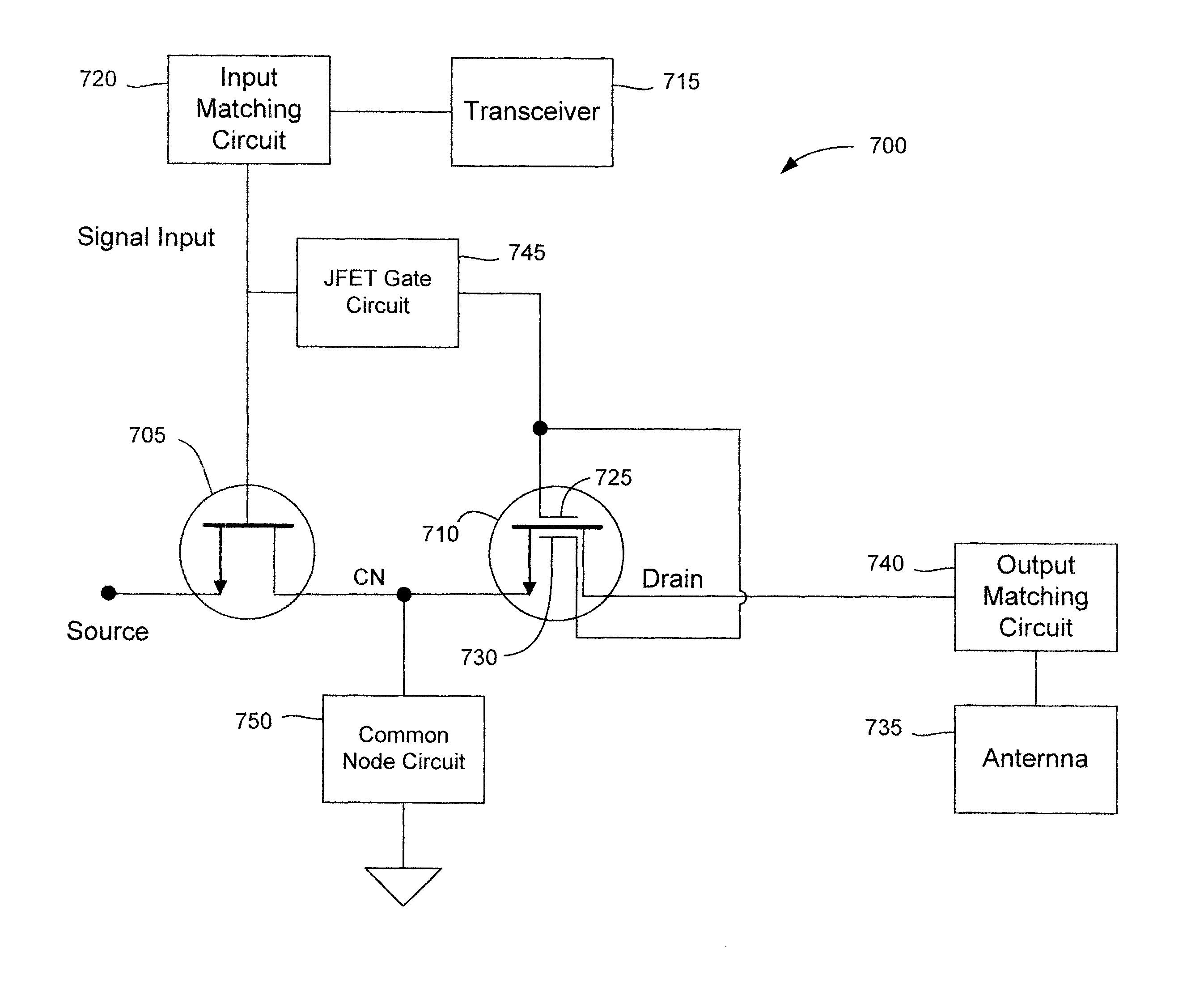
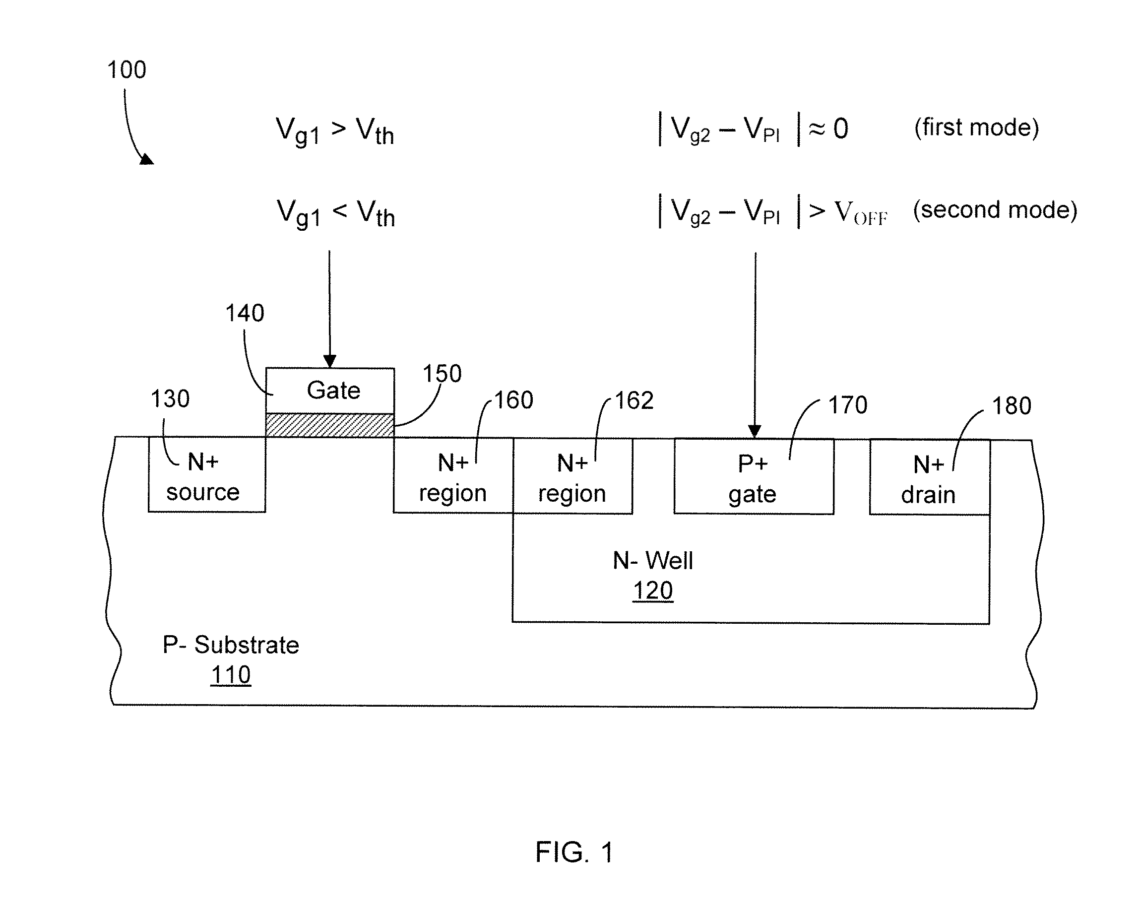
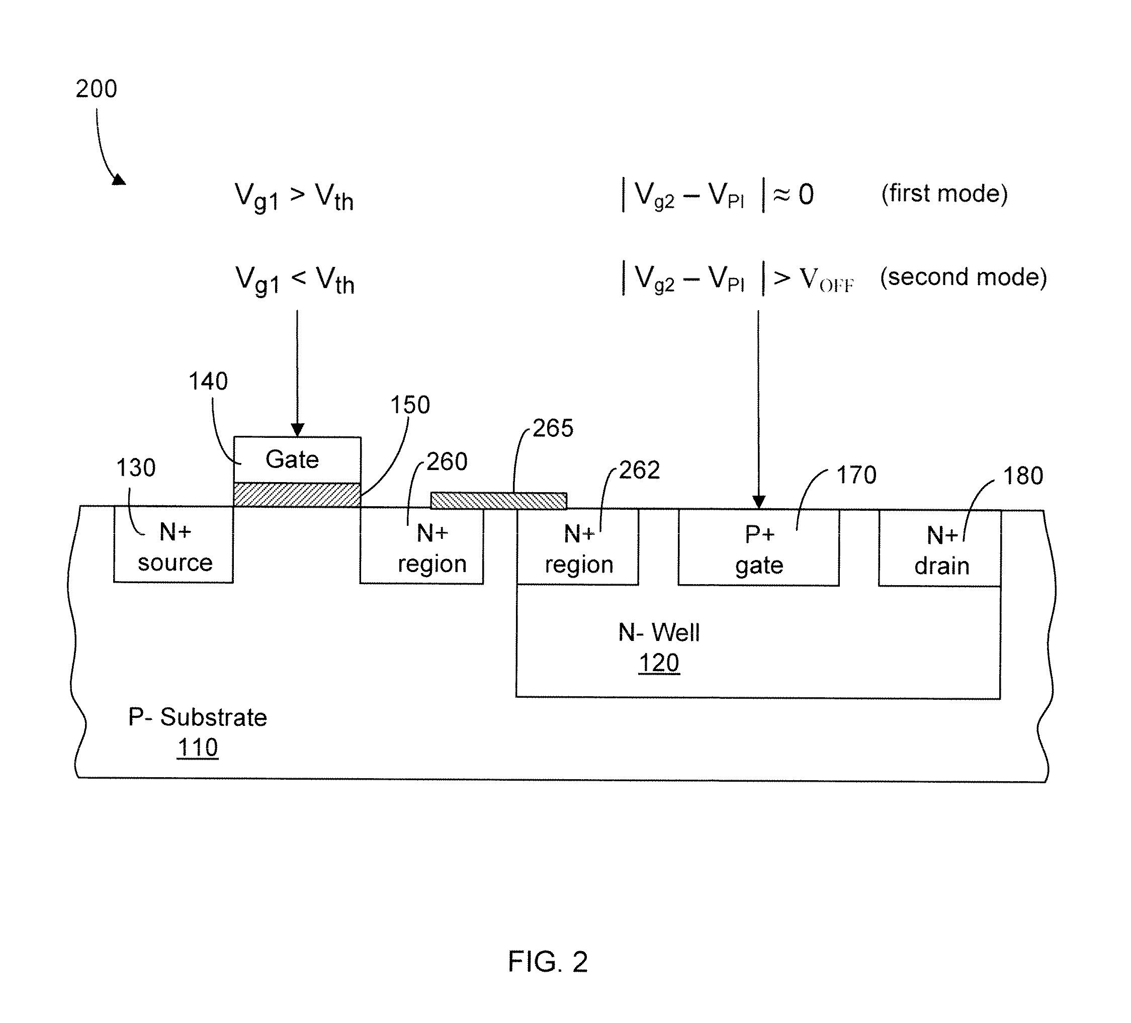
[0026]The present disclosure is directed to double-gate semiconductor devices characterized by high breakdown voltages that allow for a large excursion of the output voltage, making these semiconductor devices useful for power applications, such as power amplification. The double-gate semiconductor devices disclosed herein comprise a metal-oxide-semiconductor (MOS) gate and a junction gate, in which the bias of the junction gate may be a function of the gate voltage of the MOS gate. The breakdown voltage of such a double-gate semiconductor device is the sum of the breakdown voltages of the MOS gate and the junction gate. Because an individual junction gate has an intrinsically high breakdown voltage, the breakdown voltage of the double-gate semiconductor device is higher than the breakdown voltage of an individual MOS gate.

[0027]The double-gate semiconductor device provides improved RF capability in addition to operability at higher power levels as compared to conventional complemen...


PUM


Abstract

Electronic circuits and methods are provided for various applications including signal amplification. An exemplary electronic circuit comprises a MOSFET and a dual-gate JFET in a cascode configuration. The dual-gate JFET includes top and bottom gates disposed above and below the channel. The top gate of the JFET is controlled by a signal that is dependent upon the signal controlling the gate of the MOSFET. The control of the bottom gate of the JFET can be dependent or independent of the control of the top gate. The MOSFET and JFET can be implemented as separate components on the same substrate with different dimensions such as gate widths.

Description

CROSS-REFERENCE TO RELATED APPLICATIONS[0001]This application claims the benefit of U.S. Provisional Patent Application No. 61 / 171,689 filed on Apr. 22, 2009 and entitled “Electronic Circuits including a MOSFET and a Dual-Gate JFET and having a High Breakdown Voltage” which is incorporated herein by reference. This application is also related to U.S. patent application Ser. No. 12 / 070,019 filed on Feb. 13, 2008 and entitled “High Breakdown Voltage Double-Gate Semiconductor Device,” now U.S. Pat. No. 7,863,645 issued on Jan. 4, 2011, which is also incorporated herein by reference.BACKGROUND[0002]1. Field of Invention[0003]The present invention relates generally to semiconductor devices and more particularly to semiconductor devices configured for power applications.[0004]2. Related Art[0005]Complementary metal-oxide semiconductor (CMOS) devices designed for radio-frequency (RF) power applications have traditionally required a tradeoff between improved RF performance versus a higher b...

Claims


Application Information

Patent Timeline
Patent Type & Authority Patents(United States)
IPC IPC(8): H03F3/16
CPCH01L27/0617H03F3/195H03F3/245H03F1/223H01L27/095H01L27/098H03F3/14
Inventor BRACALE, ALEXANDRE G.MASLIAH, DENIS A.
Owner STMICROELECTRONICS INT NV
Why Eureka
Try Eureka