Multi-band multiwavelength quantum dot mode-locked lasers

a quantum dot mode-locked, multi-band technology, applied in semiconductor lasers, laser cooling arrangements, laser details, etc., can solve the problems of very limited number of lasing modes in one band, fluctuation of laser output, and inability to control the intensity of each lasing mode, etc., to achieve greater mode spacing, widen the output spectrum, and increase the wavelength separation

Active Publication Date: 2011-08-02
NAT RES COUNCIL OF CANADA
View PDF9 Cites 5 Cited by
  • Summary
  • Abstract
  • Description
  • Claims
  • Application Information

AI Technical Summary

Benefits of technology

[0081]FIG. 6a shows 6 plots of experimental lasing emission spectra taken under pump currents of 30 mA, 35 mA, 40 mA, 50 mA, 60 mA, and 70 mA, as labeled. Pth is about 17.2 mA. The pump voltage varied within about 2-4.5 volts. At each of these pump factors, a mode-locked spectral output of a single band, or dual band laser is produced. It is an advantage of the present invention that the same laser can be used for producing a single band that is mode locked, or multiple bands.
[0082]As the current increases, the output spectrum broadens. Two distinct bands can be resolved at a current of 40 mA and above. The higher the current applied across the active medium, the larger the wavelength separation between the two splitting bands caused by the AC Stark effect. In all cases the dual bands are intraband as well as interband mode locked.
[0083]At a pump current of 35 mA, a 11 channels having mode spacings of 745.2 pm was observed. The band was centered on 1554.3 nm, and had a bandwidth of (FWHM) 8.2 nm.
[0084]In contrast, at 60 mA, the laser had 15 modes, of which 10 modes were in a band from 1568 nm to 1576 nm (within the L-band), and 5 modes were in a distinct band from 1542 nm to 1546 nm (within the C-band). The 10 L-band modes had a slightly greater mode spacing at 763.0 pm, and the 5 C-band modes had a 732.4 pm mode spacing. The separation between two band center peaks at 60 mA was 28.0 nm, corresponding to a frequency difference of 3.462 THz, and the two bands were located almost symmetrically around 1557.7 nm, which coincides with the central lasing wavelength at a bias current of 30 mA.
[0085]The fact that the same laser can be made to produce a single band or pairs of bands of different separations by simply applying different currents is of considerable value.
[0086]Naturally every separation up to 28 nm can be achieved with a corresponding current between 30 and 60 mA, and greater separations (such as the 35 nm separation shown at 70 mA) are possible.Mode Locking

Problems solved by technology

Given the unavoidable fluctuations in electrical and optical fields within the optically active medium, the intracavity gain-loss balance for any lasing mode could be broken, resulting in fluctuations of the laser output.
Consequently, the number of lasing modes in one band is very limited and the intensity of each lasing mode fluctuates.
However, as far as Applicant knows, no work specially addressing two- or multi-band mode-locked lasers using QD active media has been reported.
This provides no flexibility in the positions and distributions of the bands.

Method used


Image

  • Multi-band multiwavelength quantum dot mode-locked lasers
  • Multi-band multiwavelength quantum dot mode-locked lasers
  • Multi-band multiwavelength quantum dot mode-locked lasers

Examples


experiment 1

AC Stark Splitting

Laser Diode Specification

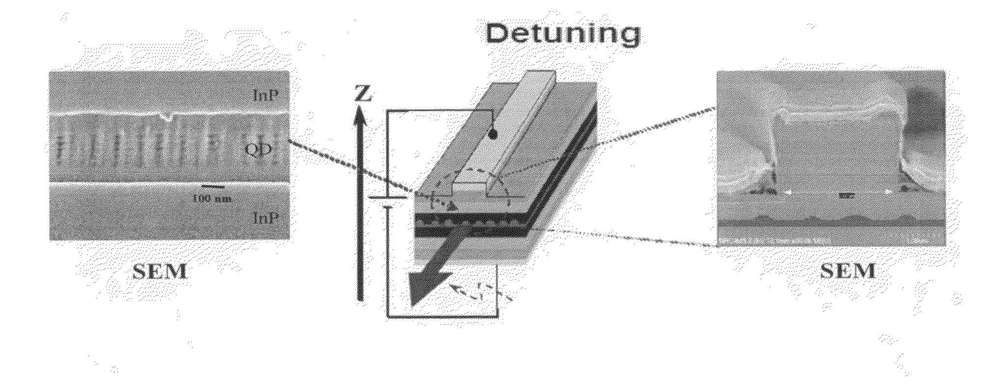
[0072]FIG. 5 shows two SEM images of an active medium used to produce a laser diode, and a schematic illustration of such a diode, according to an embodiment of the invention. The rightmost image is a high magnification SEM image of a cross-section of the active medium showing 5 stacked QD layers. The leftmost image is at a lower magnification and shows the ridge waveguide structure in cross-section. An InAs / InGaAsP active medium with a self-assembled QD was grown by chemical beam epitaxy (CBE) on exactly oriented (100) InP n-type substrates, in a manner known in the art. The undoped active regions consisted of five stacked layers of self-assembled InAs QDs embedded in quaternary In0.816Ga0.392As0.392P0.608 (1.15 Q), providing three-dimensional electron confinement.

[0073]The QDs were formed by cracking substantially planar sheets having dimensions in the neighbourhood of 10−8 m in two dimensions on average, followed by resurfacing of the pr...

example 2

Prophetic: Attenuation

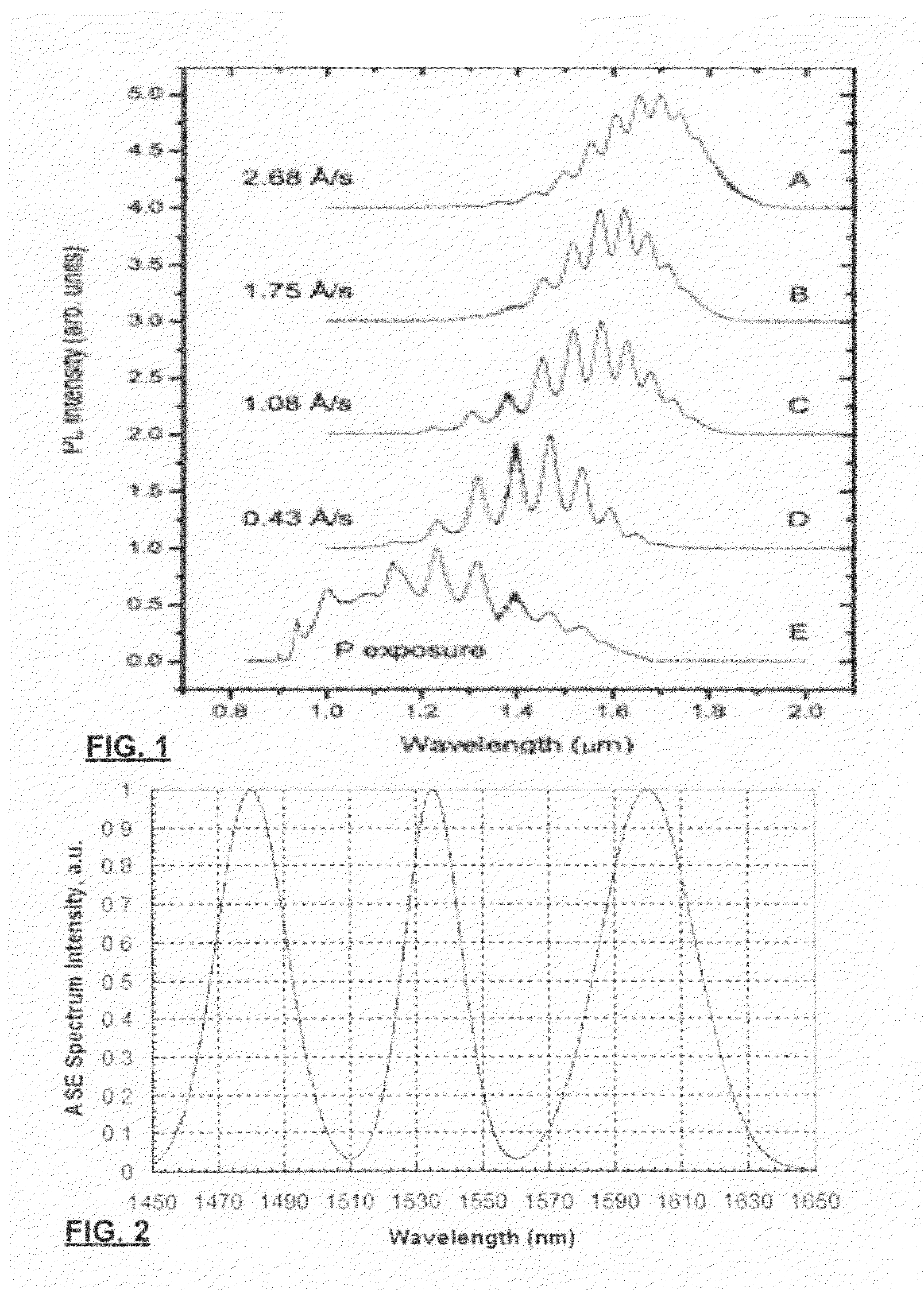
[0091]FIGS. 9a-c are graphs showing how attenuation at facets can be used to generate multi-band multiwavelength lasing. FIG. 9a is a graph of the obtained ASE spectrum of the cavity produced in relation to example 1, prior to addition of a facet. The multiwavelength channel structure is not presented as the resolution of the OSA was lower than the mode spacing. Only the band structure is manifest.

[0092]It is noted in FIG. 9a that the breadth of the uncoated ASE spectrum is great, with a FWHM of 170 nm. It is known in the art to provide cavity interfaces that selectively transmit modes as a function of frequency. Shown in FIG. 9b is a desired relative reflection spectrum designed to effectively remove modes having wavelengths of 1510-1535 nm and 1565-1585 nm from the cavity, as well as to reduce the amplitude of a center peak near 1550 nm to somewhat flatten the peak of the uncoated ASE spectrum. It is known in the art how to produce coatings to this specificat...


PUM


Abstract

A multi-band (multi-color) multiwavelength mode locked laser diode is provided by dynamic phase compensation of a quantum dot active medium. The laser diode is provided with a PIN diode structure where the active medium consists of a plurality of layers of quantum dots such as those produced by self-assembly from known chemical beam epitaxy methods. The multiplicity of bands may be produced by AC Stark splitting, frequency selective attenuation, or by the inclusion of multiple different layers having different, respective, peak ASE emissions. Dispersion compensation within laser facets, waveguides, and the optically active media permit the selection of a fixed dispersion within the cavity. A dynamic group phase change induced by the AC Stark effect permits compensation of the fixed dispersion sufficiently to produce an intraband mode-locked laser. Even interband mode locking was observed.

Description

CROSS-REFERENCE TO RELATED APPLICATIONS[0001]This application claims the benefit of U.S. Provisional patent application Ser. No. 61 / 136,698 filed Sep. 25, 2008; and Canadian Formal Application 2,674,959 filed Jun. 25, 2009 the entire contents of which is herein incorporated by reference.FIELD OF THE INVENTION[0002]This invention relates in general to optical laser sources such as may be used in telecommunications, optical networking systems, sensing, metrology, instrumentation, spectroscopy, imaging, laser machining, and RF / THz generators. More particularly the invention relates to the use of nonlinear effects of quantum dot active media to produce two or more multiwavelength bands that are intraband mode locked, or even mutually (interband) mode locked.BACKGROUND OF THE INVENTION[0003]Multiwavelength lasers based on Quantum Dots (QDs) are known in the art. They produce light that, in the frequency domain, consists of a few to hundreds of lasing modes that are discretely and substan...

Claims


Application Information

Patent Timeline
Patent Type & Authority Patents(United States)
IPC IPC(8): H01S3/098H01S3/10
CPCB82Y20/00H01S5/065H01S5/0657H01S5/3412
Inventor LIU, JIARENLU, ZHENGUORAYMOND, SYLVAINPOOLE, PHILIPBARRIOS, PEDROPOITRAS, DANIEL
Owner NAT RES COUNCIL OF CANADA
Why Eureka
Try Eureka