Multi-band multiwavelength quantum dot mode-locked lasers
a quantum dot mode-locked, multi-band technology, applied in semiconductor lasers, laser details, electrical devices, etc., can solve the problems of very limited number of lasing modes in one band, fluctuation of laser output, and very large laser output frequency, so as to achieve greater mode spacing, widen output spectrum, and large wavelength separation
- Summary
- Abstract
- Description
- Claims
- Application Information
AI Technical Summary
Benefits of technology
Problems solved by technology
Method used
Image
Examples
experiment 1
AC Stark Splitting
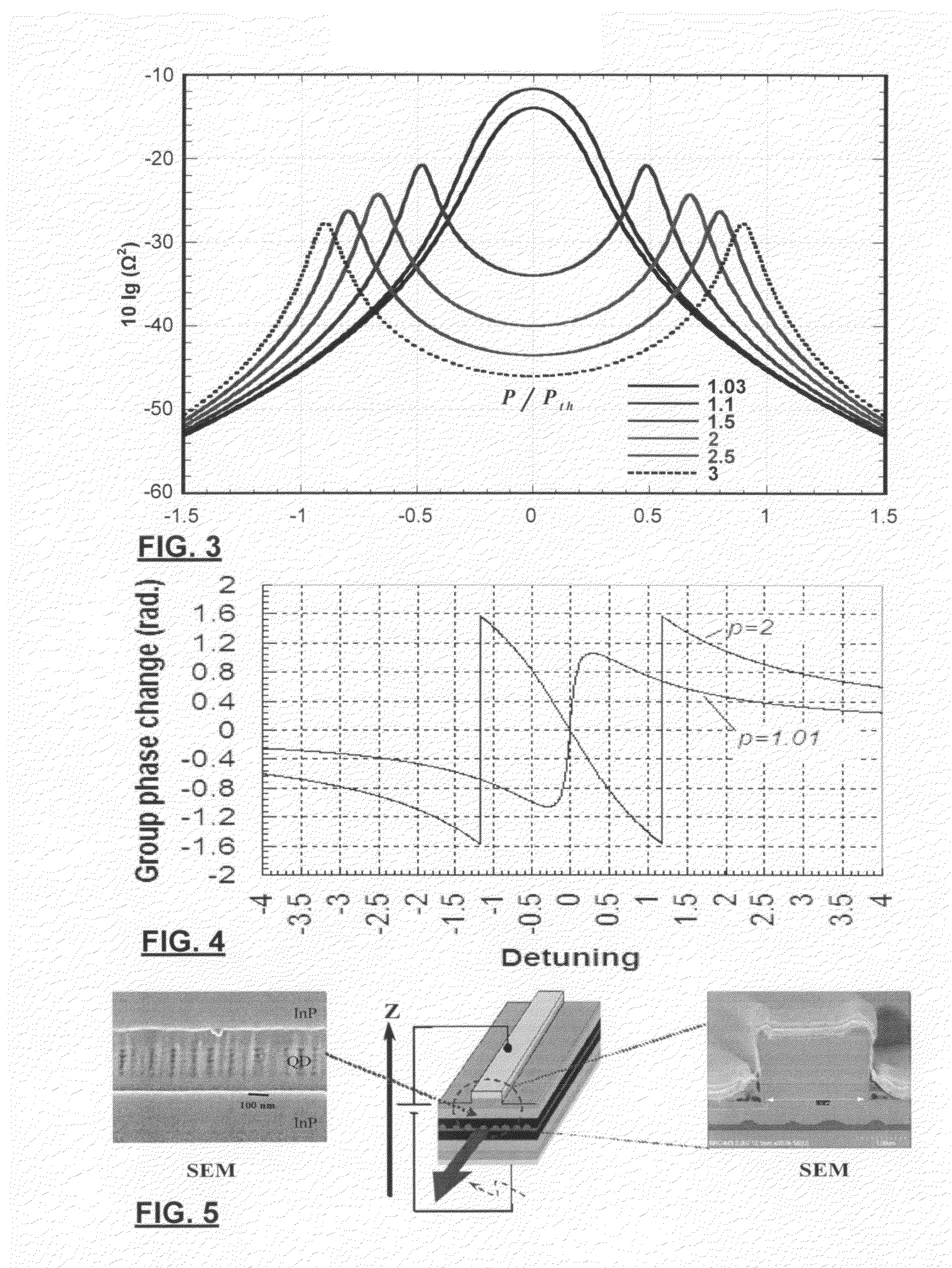
[0071]FIG. 5 shows two SEM images of an active medium used to produce a laser diode, and a schematic illustration of such a diode, according to an embodiment of the invention. The rightmost image is a high magnification SEM image of a cross-section of the active medium showing 5 stacked QD layers. The leftmost image is at a lower magnification and shows the ridge waveguide structure in cross-section. An InAs / InGaAsP active medium with a self-assembled QD was grown by chemical beam epitaxy (CBE) on exactly oriented (100) InP n-type substrates, in a manner known in the art. The undoped active regions consisted of five stacked layers of self-assembled InAs QDs embedded in quaternary In0.816Ga0.392As0.392P0.608 (1.15 Q), providing three-dimensional electron confinement.
[0072]The QDs were formed by cracking substantially planar sheets having dimensions in the neighbourhood of 10−8 m in two dimensions on average, followed by resurfacing of the pr...
example 2
Prophetic
Attenuation
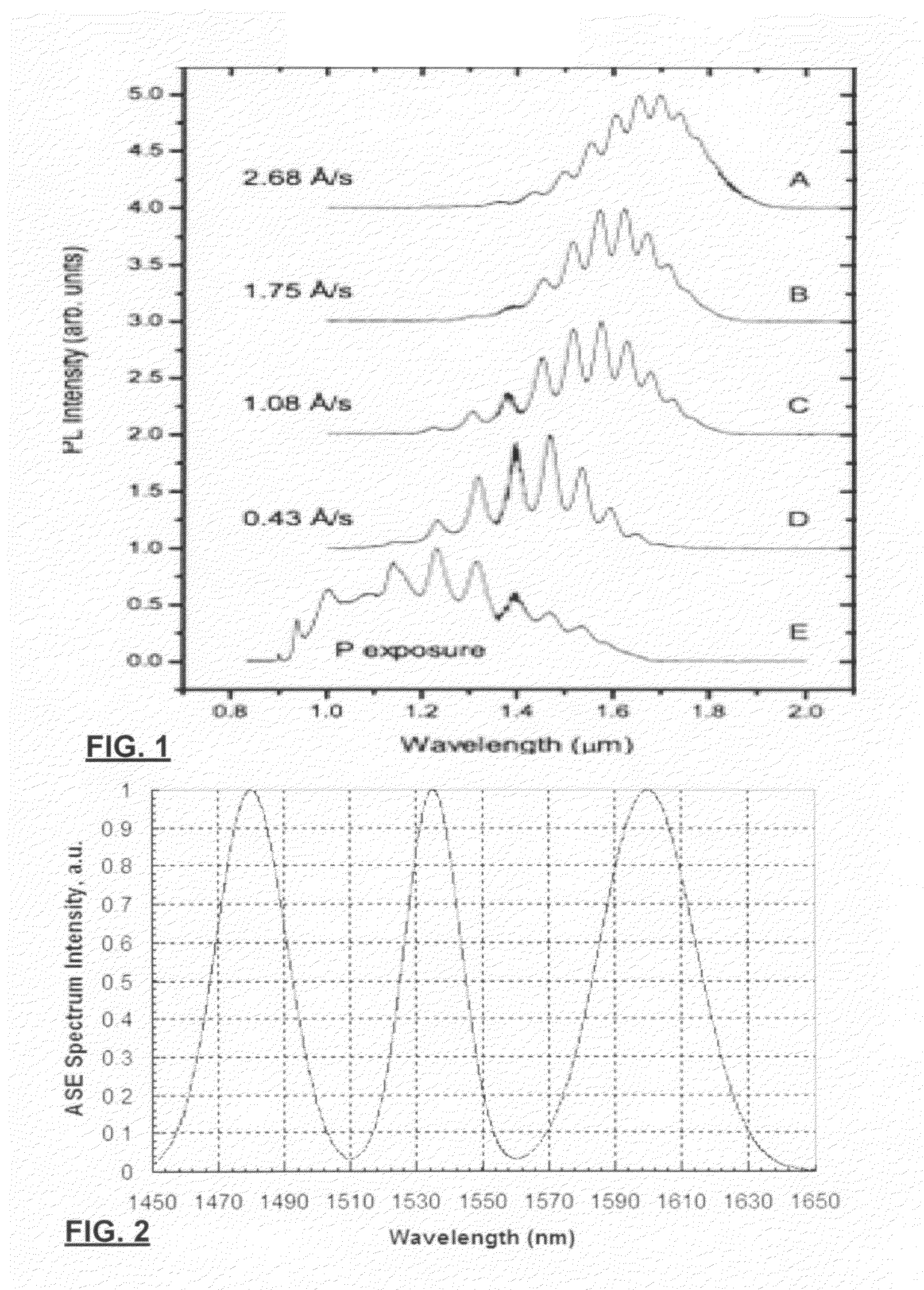
[0090]FIGS. 9a-c are graphs showing how attenuation at facets can be used to generate multi-band multiwavelength lasing. FIG. 9a is a graph of the obtained ASE spectrum of the cavity produced in relation to example 1, prior to addition of a facet. The multiwavelength channel structure is not presented as the resolution of the OSA was lower than the mode spacing. Only the band structure is manifest.
[0091]It is noted in FIG. 9a that the breadth of the uncoated ASE spectrum is great, with a FWHM of 170 nm. It is known in the art to provide cavity interfaces that selectively transmit modes as a function of frequency. Shown in FIG. 9b is a desired relative reflection spectrum designed to effectively remove modes having wavelengths of 1510-1535 nm and 1565-1585 nm from the cavity, as well as to reduce the amplitude of a center peak near 1550 nm to somewhat flatten the peak of the uncoated ASE spectrum. It is known in the art how to produce coatings to this specificatio...
PUM
 Abstract
Description
Claims
Application Information


