
Semiconductor light receiving device

a technology of light receiving device and semiconductor, applied in the direction of semiconductor devices, basic electric elements, electrical appliances, etc., can solve the problems of increasing the dark current, the initial characteristics are degraded with certain possibility, and the responsiveness of the device might deteriorate, so as to achieve high speed and high sensitivity characteristics, the effect of high resistance to light inpu

Inactive Publication Date: 2011-08-09
NEC CORP
View PDF9 Cites 2 Cited by
  • Summary
  • Abstract
  • Description
  • Claims
  • Application Information

AI Technical Summary

Benefits of technology

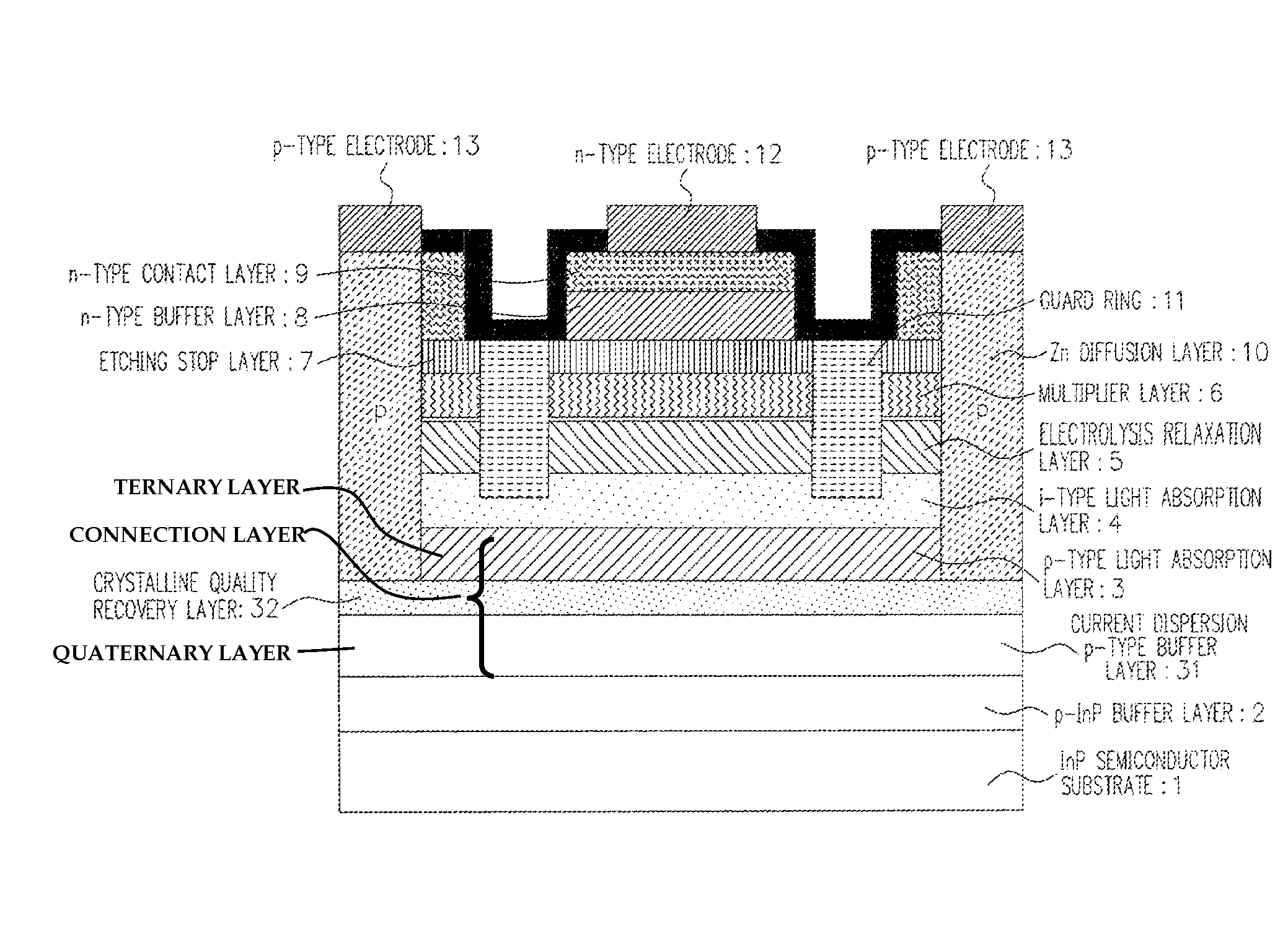
The present invention provides a semiconductor light receiving device with improved performance. The device includes a light absorption layer and a quaternary buffer layer between the InP semiconductor substrate and the light absorption layer. The quaternary buffer layer contains a quaternary compositional material that matches the lattice structure of InP, and the layer thickness of the quaternary buffer layer is 0.5 μm or greater. The device also includes a current dispersion layer that disperses current distribution, and the concentration gradient structure of the current dispersion layer is high concentration on the side of the InP semiconductor substrate and low concentration on the side of the light absorption layer. The bandgap energy of the current dispersion layer satisfies a relational expression, and the concentration gradient structure has a ratio within a range defined by R2(Nb / Na) between 10 and ∞. The device also includes a crystalline quality recovery layer that divides a connection layer made of a ternary compositional material and a quaternary compositional material, and the layer thickness of the crystalline quality recovery layer is within the range of 10 nm to 100 nm. The invention provides a semiconductor light receiving device with improved performance by incorporating these features.

Problems solved by technology

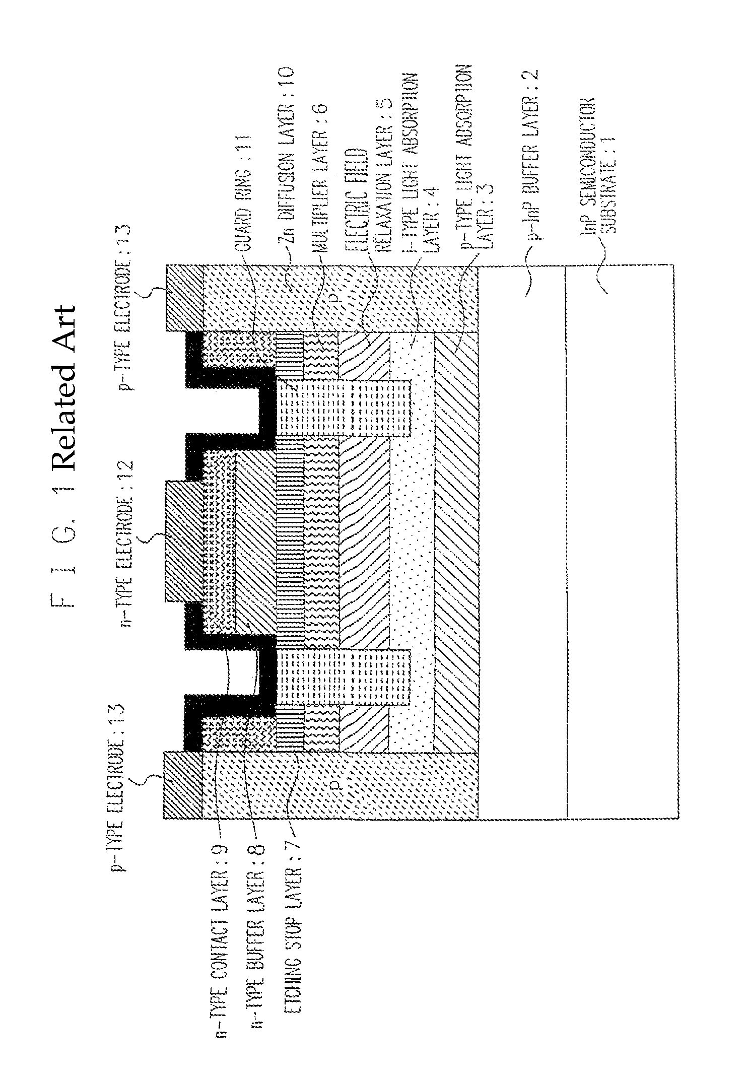
However, it has become apparent that the device responsiveness might deteriorate when there is a very intensive light input to the semiconductor light receiving device show in FIG. 1.
In some devices, however, the initial characteristics are degraded with certain possibility.
More specifically, there might be an increase in dark current, and a short-circuit failure might be caused.
However, unlike the technique according to the present invention, the above described technique is not designed to solve the deterioration of the responsiveness of the device when there is a very intensive light input.
However, Patent Document 1 does not suggest any solution for the problem of the deterioration of the device responsiveness caused when a very intensive light is input.

Method used


Image

  • Semiconductor light receiving device
  • Semiconductor light receiving device
  • Semiconductor light receiving device

Examples


first exemplary embodiment

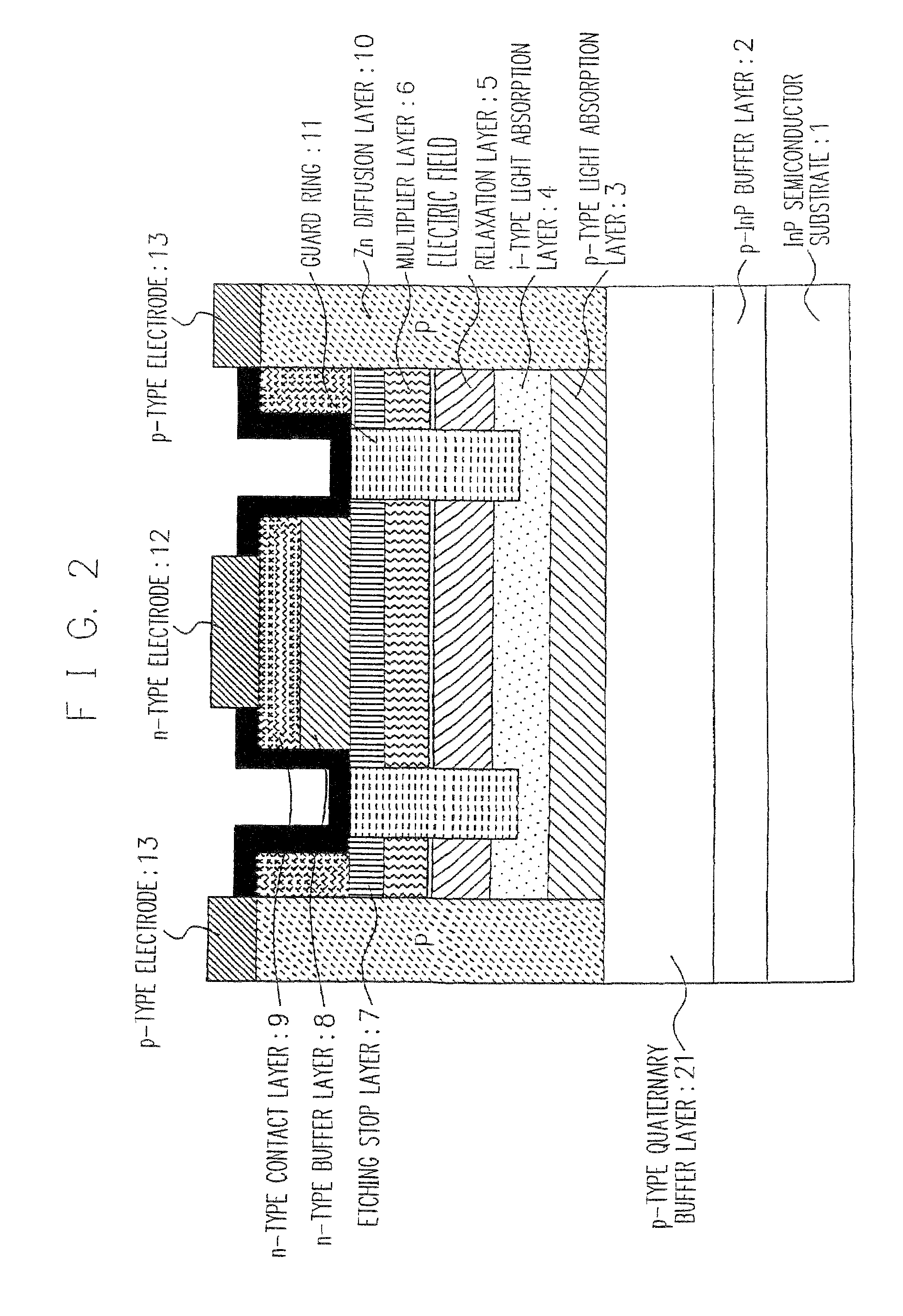
[0051]Referring first to FIG. 2, the structure of the semiconductor light receiving device of the exemplary embodiment is described.

[0052]As shown in FIG. 2, the semiconductor light receiving device of the exemplary embodiment includes an InP semiconductor substrate (1), a p-InP buffer layer (2), a p-type quaternary buffer layer (21), a p-type light absorption layer (3), an i-type light absorption layer (4), an electric field relaxation layer (5), a multiplier layer (6), an etching stop layer (7), an n-type buffer layer (8), and an n-type contact layer (9).

[0053]In the semiconductor light receiving device of the exemplary including the layer structure shown in FIG. 2, the n-type contact layer (9) and the n-type buffer layer (8) are removed around a light receiving part from the above, until the removal reaches the etching stop layer (7). Ti ions are then implanted to form a guard ring (11). Zn diffusion is then caused in the neighboring area of the guard ring (11), so as to form a Z...

example 1 of first exemplary embodiment

[0077]Referring to FIG. 2, a first example structure of the semiconductor light receiving device of the first exemplary embodiment is now described.

[0078]As shown in FIG. 2, the semiconductor light receiving device of the exemplary embodiment includes the stack structure formed on the InP semiconductor substrate (1). The stack structure includes the p-InP buffer layer (2), the p-type quaternary buffer layer (21), the p-type light absorption layer (3), the i-type light absorption layer (4), the electric field relaxation layer (5), the multiplier layer (6), the etching stop layer (7), the n-type buffer layer (8), and the n-type contact layer (9) stacked in this order. The n-type contact layer (9) and the n-type buffer layer (8) are removed around the light receiving part until the removal reaches the etching stop layer (7). Ti ions are then implanted to form the guard ring (11). After a dielectric film is formed, Zn diffusion is caused in the neighboring area of the guard ring (11) to...

example 2 of first exemplary embodiment

[0080]Referring now to FIG. 4, a second example structure of the semiconductor light receiving device of the first exemplary embodiment is described.

[0081]As shown in FIG. 4, the semiconductor light receiving device of the exemplary embodiment includes the stack structure formed on an InP semiconductor substrate (1). The stack structure includes the p-InP buffer layer (2), the p-type quaternary buffer layer (21), the crystalline quality recovery layer (22), the p-type light absorption layer (3), the i-type light absorption layer (4), the electric field relaxation layer (5), the multiplier layer (6), the etching stop layer (7), the n-type buffer layer (8), and the n-type contact layer (9) stacked in this order. The n-type contact layer (9) and the n-type buffer layer (8) are removed around the light receiving part until the removal reaches the etching stop layer (7). Ti ions are then implanted to form the guard ring (11). After a dielectric film is formed, Zn diffusion is caused in t...


PUM


Abstract

The present invention provides a semiconductor light receiving device that prevents local heat generation, has high-speed, high-sensitivity characteristics even at the time of an intensive light input, and exhibits high resistance to light inputs. The semiconductor light receiving device includes light absorption layers (3, 4) formed on an InP semiconductor substrate (1) wherein a buffer layer (21) containing a quaternary compositional material is formed between the InP semiconductor substrate (1) and the light absorption layers (3, 4).

Description

FIELD OF THE INVENTION[0001]The present invention relates to a semiconductor light receiving device, and more particularly, to a semiconductor light receiving device that has excellent high-frequency characteristics.BACKGROUND OF THE INVENTION[0002]There are various kinds of semiconductor light receiving device. Among them, APD (Avalanche Photo Diodes) are devices that exhibit particularly high light-receiving sensitivity, including a multiplier function.[0003]APD can be roughly classified into a group of devices made of Si and a group of devices formed with compound semiconductors. The devices containing compound semiconductors can be further classified into a group of devices containing GaAs as a substrate and a group of devices containing InP as a substrate. In terms of structures, those devices can be classified into a planar type or a mesa type.[0004]Based on the differences in layer structure and carrier multiplying structure, those devices can be also classified into an elect...

Claims


Application Information

Patent Timeline
Patent Type & Authority Patents(United States)
IPC IPC(8): H01L31/07
CPCH01L31/107
Inventor NAKATA, TAKESHI
Owner NEC CORP
Learn More