Organic el device and method of producing the device

a technology of organic el and electrodes, which is applied in the manufacture of electrode systems, electric discharge tubes/lamps, and discharge tubes luminescent screens, etc., can solve the problems of affecting the el device's el performance, affecting the el performance, so as to prevent the infiltration of moisture or oxygen into the organic compound layer of the organic el devi

Active Publication Date: 2011-08-09
CANON KK
View PDF8 Cites 6 Cited by
  • Summary
  • Abstract
  • Description
  • Claims
  • Application Information

AI Technical Summary

Benefits of technology

[0014]An object of the present invention is to provide an organic EL device having the following characteristics and a method of producing the device: voids generated in a production process for the organic EL device can be suppressed, and the infiltration of moisture or oxygen into the organic compound layer of the organic EL device can be prevented.
[0016]According to the present invention, voids generated in a production process for an organic EL device can be suppressed, and the infiltration of moisture or oxygen into the organic compound layer of the organic EL device can be prevented.

Problems solved by technology

The organic EL device is liable to cause the degradation of characteristics owing to moisture or oxygen, the organic compound layer is peeled from an electrode layer owing to a trace amount of moisture, and the peeling is responsible for the occurrence of a dark spot.
Further, the void may swell to burst.
However, foreign matter such as a cluster generated upon formation of the organic compound layer of the organic EL device by vapor deposition or the etching residue of a device isolation film adheres onto the organic EL device.
The passivation layer formed of a silicon nitride film or an ITO film formed with a vapor deposition method or a sputtering method is a hard film having insufficient coverage performance, so the layer cannot completely cover the above foreign matter when the layer is formed on the foreign matter.
In addition, an increase in thickness of the layer involves, for example, the following problems: a crack is generated in the layer as a sealing film, or the sealing film splinters.
Accordingly, the layer does not suffice for the prevention of the infiltration of moisture or oxygen into the device.

Method used


Image

  • Organic el device and method of producing the device
  • Organic el device and method of producing the device
  • Organic el device and method of producing the device

Examples


example 1

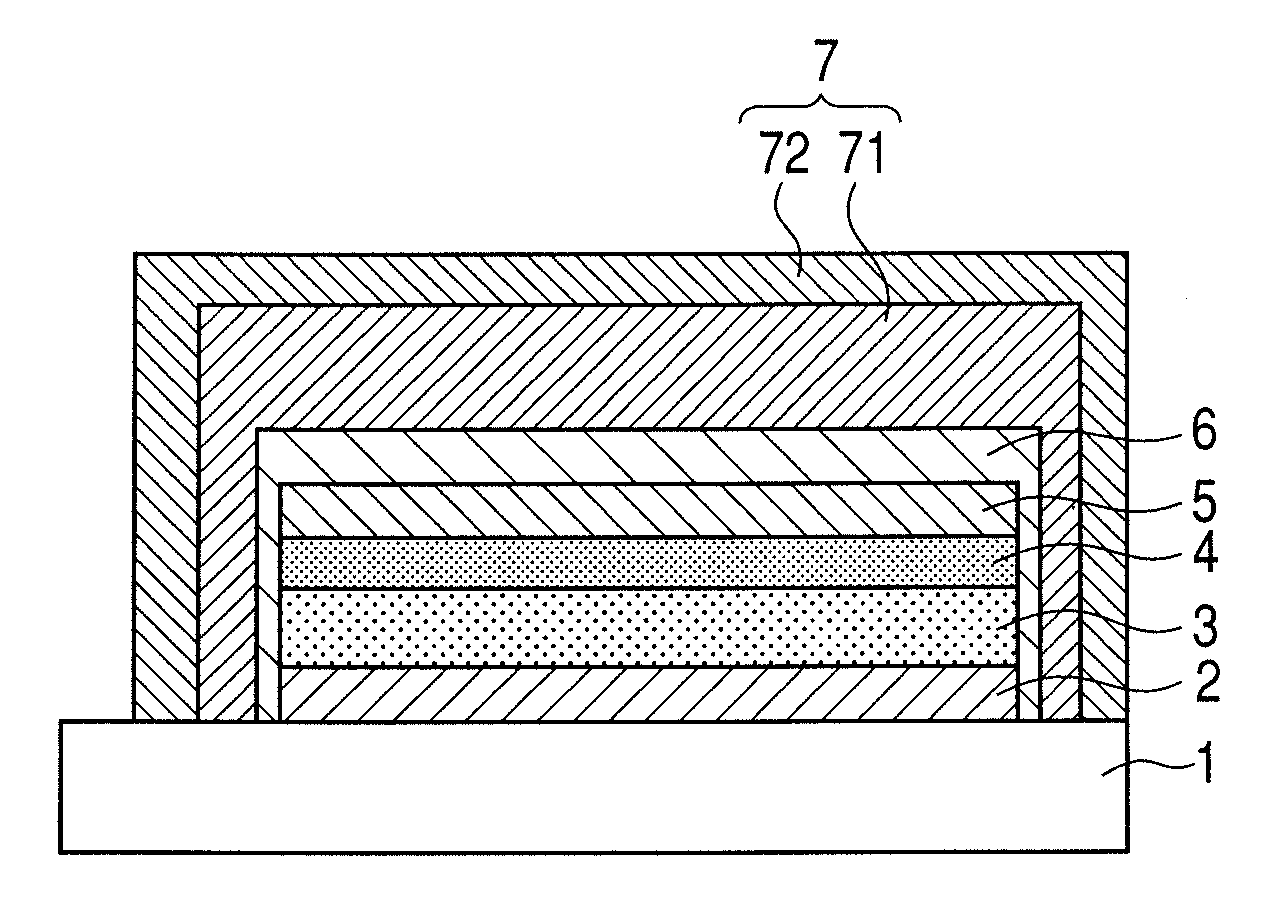
[0051]The generation of voids in the organic EL device of the present invention shown in FIG. 1 is evaluated.

[0052]The substrate 1 having a constitution shown in FIG. 1 is formed by stacking a TFT, an insulating film, and an organic planarization film (none of which is shown) in the stated order on a glass substrate. The lower electrode 2 formed of chromium is formed on the substrate, and furthermore, the periphery of the electrode is insulated with a device isolation film formed of polyimide (not shown).

[0053]First, the above substrate 1 was baked in a vacuum baking furnace at 200° C. for 4 hours. After that, the pressure in the vacuum baking furnace was returned to atmospheric pressure, and the substrate was taken out of the vacuum baking furnace and conveyed. Next, the substrate was placed in a baking chamber. The chamber was evacuated to a degree of vacuum of 1×10⁻⁴ Pa, and the substrate was baked at 150° C. for 10 minutes. The substrate 1 was conveyed to a UV chamber. The press...

example 2

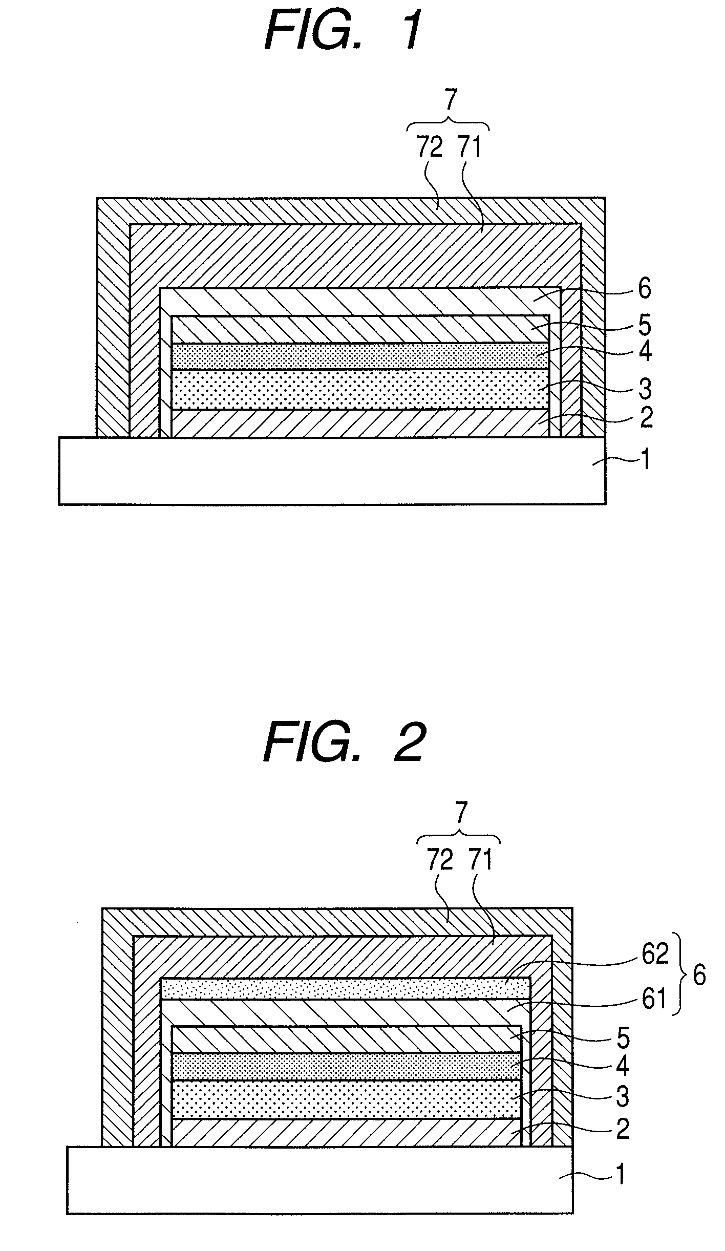
[0064]In Example 2, an organic EL device shown in FIG. 1 was produced while silicon oxide was used in the first passivation layer 6 and the thickness of the first passivation layer 6 was changed.

[0065]The same substrate as that of Example 1 was used, and a process commencing on vacuum baking to ending on the formation of the upper electrode was the same as that of Example 1.

[0066]The substrate was conveyed to another sputtering chamber, and silicon oxide was formed into a film having on the substrate with a DC sputtering method while oxygen and an argon gas were flowed and the pressure at which the film was formed was adjusted to 0.8 Pa, whereby the first passivation layer 6 was obtained.

[0067]The second passivation layer 7 was formed in the same manner as in Example 1.

[0068]The above process was repeated so that three organic EL devices in each of which the thickness of the first passivation layer 6 was 50 nm, three organic EL devices in each of which the thickness of the layer was...

example 3

[0079]In Example 3, an organic EL device shown in FIG. 2 was produced while silicon oxide was used in the first layer 61 of the first passivation layer 6, silicon nitride was used in the second layer 62 of the layer, and the thickness of each of the first and second layers was changed.

[0080]The same substrate 1 as that of Example 1 was used, and a process commencing on vacuum baking to ending on the formation of the upper electrode 2 was the same as that of Example 1.

[0081]The substrate 1 was conveyed to another sputtering chamber, and silicon oxide was formed into a film on the substrate with a DC sputtering method by using a target formed of silicon while oxygen and an argon gas were flowed and the pressure at which the film was formed was adjusted to 0.8 Pa, whereby the first layer 61 of the first passivation layer 6 was obtained.

[0082]The substrate 1 was conveyed to another sputtering chamber, and silicon nitride was formed into a film on the substrate with a DC sputtering metho...


PUM

PropertyMeasurementUnit
thicknessaaaaaaaaaa
thicknessaaaaaaaaaa
thicknessaaaaaaaaaa

Abstract

Provided is an organic EL device including a substrate, a lower electrode, an organic compound layer containing one of an alkali metal and an alkali metal compound, an upper electrode formed of an oxide film, and passivation layers for covering the lower electrode, the organic compound layer, and the upper electrode, the lower electrode, the organic compound layer, the upper electrode, and the passivation layers being stacked in the stated order on the substrate, in which the passivation layers include a first passivation layer formed on the upper electrode, which contains silicon as a main component, and which is free of hydrogen and a second passivation layer formed on the first passivation layer which contains silicon as a main component and hydrogen.

Description

BACKGROUND OF THE INVENTION[0001]1. Field of the Invention[0002]The present invention relates to an organic electroluminescence (EL) device for use in, for example, a flat panel display, and a method of producing the device.[0003]2. Description of the Related Art[0004]An organic EL device being a self light-emitting device as a flat panel display has been recently attracting attention. The organic EL device is liable to cause the degradation of characteristics owing to moisture or oxygen, the organic compound layer is peeled from an electrode layer owing to a trace amount of moisture, and the peeling is responsible for the occurrence of a dark spot. In view of the foregoing, the organic EL device is covered with an etching glass cover, a sealing agent is used to bond the periphery of the resultant, and the inside of the resultant is attached with a moisture absorbent so that moisture infiltrating from a sealing surface is absorbed by the moisture absorbent. As a result, the lifetime...

Claims


Application Information

Patent Timeline
Patent Type & Authority Patents(United States)
IPC IPC(8): H01L51/50
CPCH01L51/5092H01L51/5237H10K50/171H10K50/841H10K50/8426H10K50/844H10K50/86H10K2102/3026
Inventor AOTA, YUKITO
Owner CANON KK
Why Eureka
Try Eureka