Insulating transformer and power conversion device
a technology of transformer and power conversion device, which is applied in the direction of transformer/inductance coil/winding/connection, electronic switching, pulse technique, etc., can solve the problems the difficulty of satisfying the demands of continuous operation for ten years or longer in high-temperature environments, and the occurrence of dielectric breakdown of the separation layer 59/b>, so as to improve reliability and environmental tolerance. , the effect of improving the toleran
- Summary
- Abstract
- Description
- Claims
- Application Information
AI Technical Summary
Benefits of technology
Problems solved by technology
Method used
Image
Examples
first embodiment
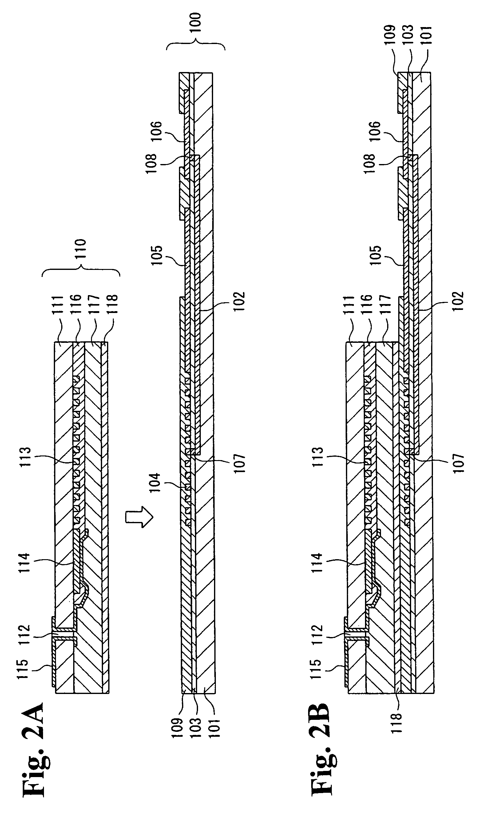
[0122]FIGS. 2A, 2B are cross-sectional views briefly showing the configuration of the insulating transformer of the invention.
[0123]In FIGS. 2A, 2B, the insulating transformer is provided with a primary-side coil 110, formed on an insulating substrate 111, and with a secondary-side coil 100, formed on a semiconductor substrate 101.
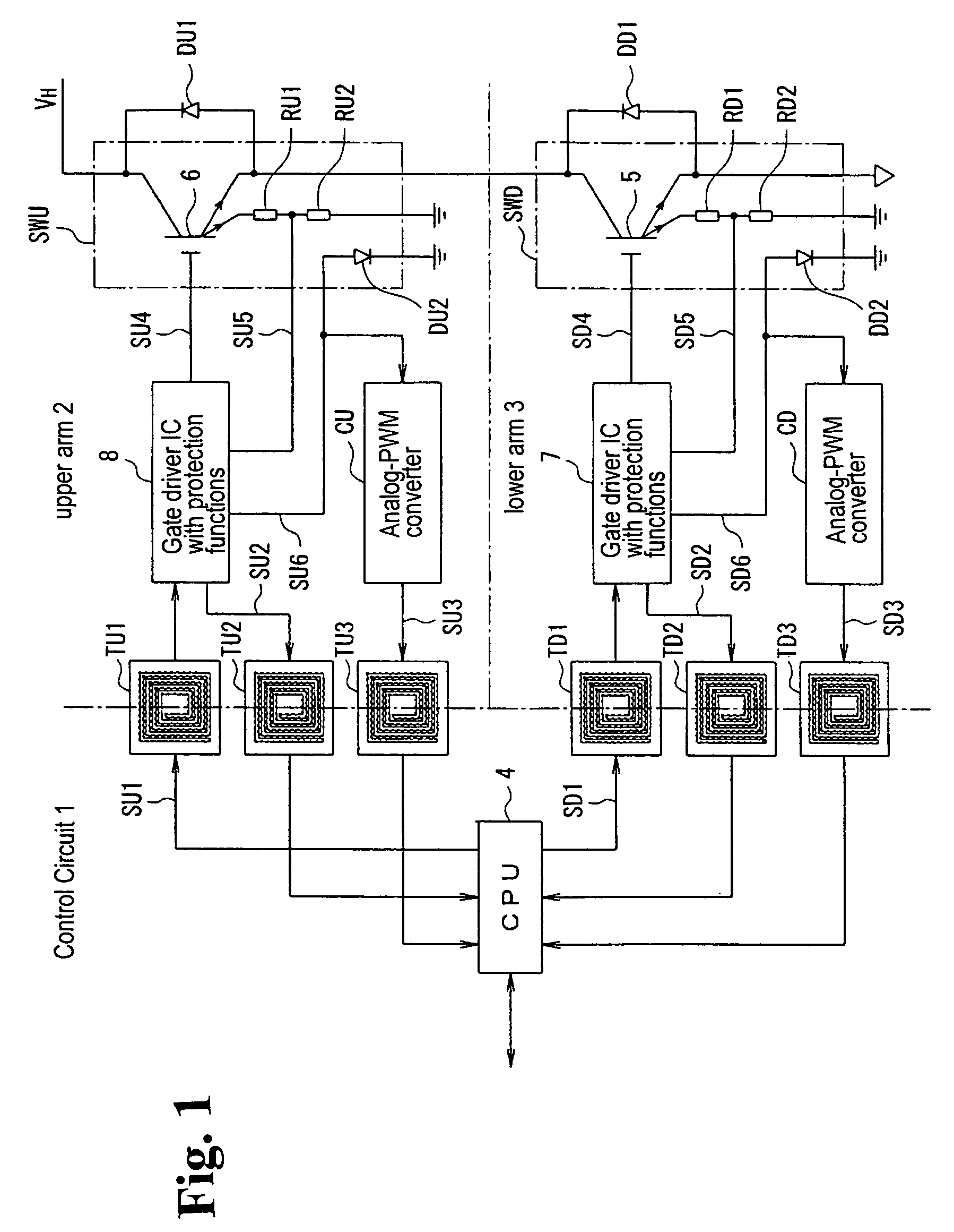
[0124]Here, in the secondary-side coil 100, a lead wire layer 102 is buried in the semiconductor substrate 101, and the secondary coil pattern 104 and electrodes patterns 105, 106 are formed on the semiconductor substrate 101, with an insulating layer 103 intervening. The gate driver ICs 7 and 8 with protection functions, analog-PWM converters CU and CD, and other integrated circuitry, or the switching elements SWU and SWD, and similar shown in FIG. 1 may be formed on the semiconductor substrate 101. The material of the semiconductor substrate 101 can, for example, be selected from among Si, Ge, SiGe, SiC, SiSn, PbS, GaAs, InP, GaP, GaN, ZnSe, or similar. ...
second embodiment
[0152]FIG. 5 is a cross-sectional view briefly showing the configuration of the primary-side coil of the insulating transformer of the invention.
[0153]In FIG. 5, a primary coil pattern 213 and electrode pattern 214 are formed on a first main face of an insulating substrate 211, and the primary coil pattern 213 and electrode pattern 214 are covered by an insulating layer 216 so as to expose the connection surface of the electrode pattern 214. As the insulating substrate 211, for example, a glass plate, ceramic substrate, resin substrate, or similar can be used. Alternatively, a Si substrate or other semiconductor substrate may be used. When the material of the insulating substrate 211 does not have insulating properties, an insulating layer may be formed on the surface so as to provide the substrate with insulating properties.
[0154]On the other hand, an electrode pattern 215 for wire extraction is formed on the second main face of the insulating substrate 211 opposite to the first ma...
PUM
| Property | Measurement | Unit |
|---|---|---|
| voltage | aaaaa | aaaaa |
| voltage | aaaaa | aaaaa |
| outer diameter | aaaaa | aaaaa |
Abstract
Description
Claims
Application Information


