Display device having pixel including transistor and driving method of the same

a technology of a display device and a driving method, which is applied in the direction of static indicating devices, instruments, electroluminescent light sources, etc., can solve the problems of long writing time, insufficient writing time for writing a slight amount of current, and limited capacitance of two capacitors, etc., to achieve accurate writing, shorten writing time, and improve image quality

Inactive Publication Date: 2011-08-09
SEMICON ENERGY LAB CO LTD
View PDF27 Cites 10 Cited by
  • Summary
  • Abstract
  • Description
  • Claims
  • Application Information

AI Technical Summary

Benefits of technology

[0020]Switches of various modes can be used as a switch described in the invention. For example, an electrical switch, a mechanical switch, or the like can be used. That is, it may be anything as far as it can control a current flow. It may be a transistor, a diode (for example, a PN diode, a PIN diode, a Schottky diode, a diode-connected transistor, and the like), a thyristor, or a logic circuit configured with them. Therefore, in the case of applying a transistor as a switch, polarity (conductivity type) thereof is not particularly limited because it operates just as a switch. However, when an off current is preferred to be small, a transistor of polarity with a smaller off current is favorably used. For example, the transistor which is provided with an LDD region, a transistor which has a multi-gate structure, or the like has a small off current. Further, it is desirable that an n-channel transistor is employed when a potential of a source terminal of the transistor as a switch is closer to the low potential side power source potential (Vss, GND, 0 V or the like), and a p-channel transistor is desirably employed when the potential of the source terminal is closer to the high potential side power source potential (Vdd or the like). This helps the switch operate efficiently as an absolute value of a gate-source voltage of the transistor can be increased.
[0056]In the invention, a writing period can be shortened by simultaneously obtaining a threshold voltage of a driving transistor and writing a video signal in a writing period of the video signal. As a result, a writing period per pixel can be set longer, thereby a video signal can be more accurately written and an organic EL display with higher image quality can be provided. Moreover, as a video signal can be written to more pixels in the same writing period, a large EL display and an EL display with higher resolution can be provided.

Problems solved by technology

As time to charge parasitic capacitance of a source signal line or the like is required to input a slight amount of current as a video signal to a pixel, there is a problem in that long writing time is required.
As an area of one pixel is limited, the capacitance of two capacitors are also limited.
Therefore, there is a problem in that there is not enough writing time for writing a slight amount of current as a video signal, and in a large panel in particular, a writing period per pixel becomes shorter as compared to a small panel.

Method used


Image

  • Display device having pixel including transistor and driving method of the same
  • Display device having pixel including transistor and driving method of the same
  • Display device having pixel including transistor and driving method of the same

Examples


embodiment mode 1

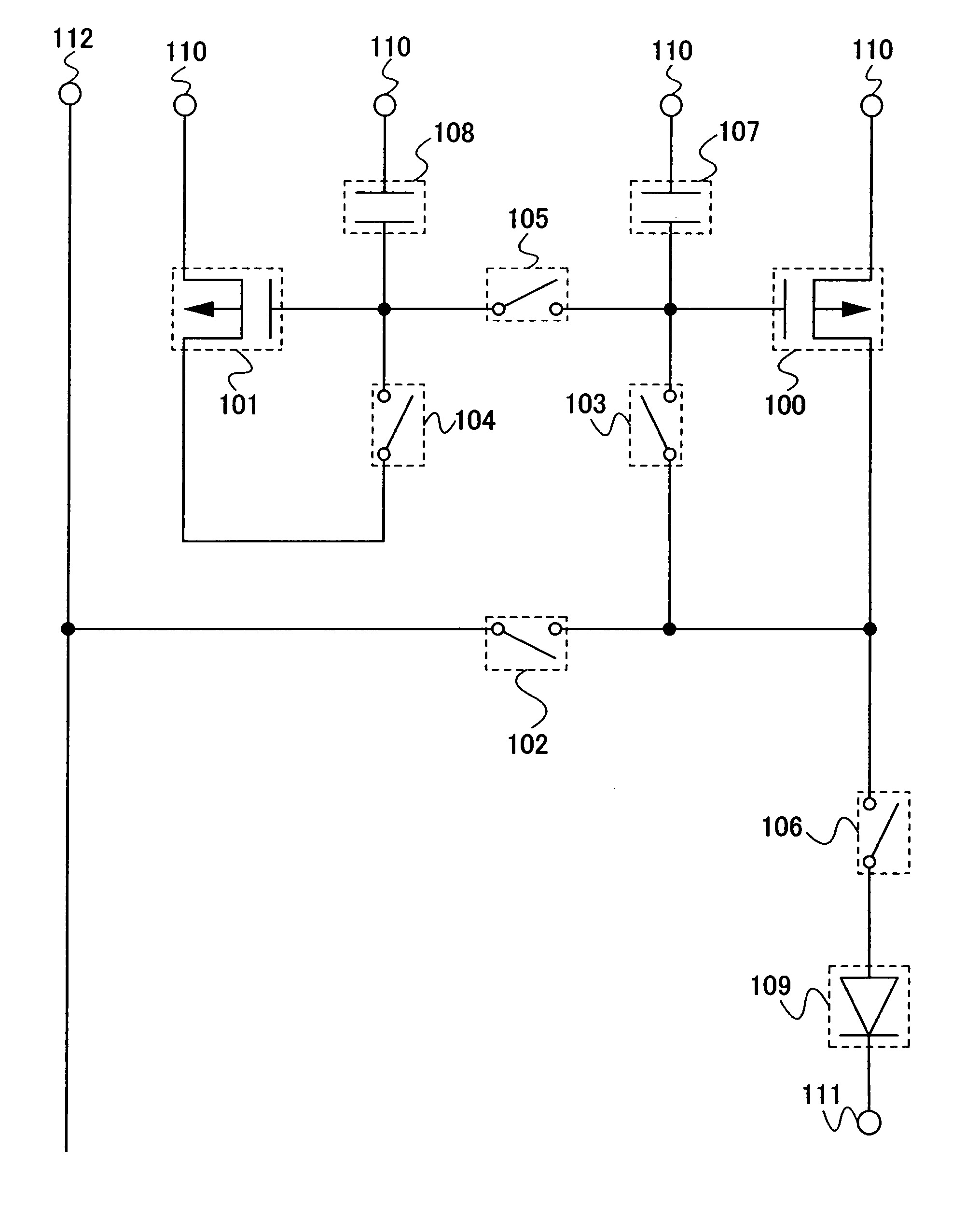
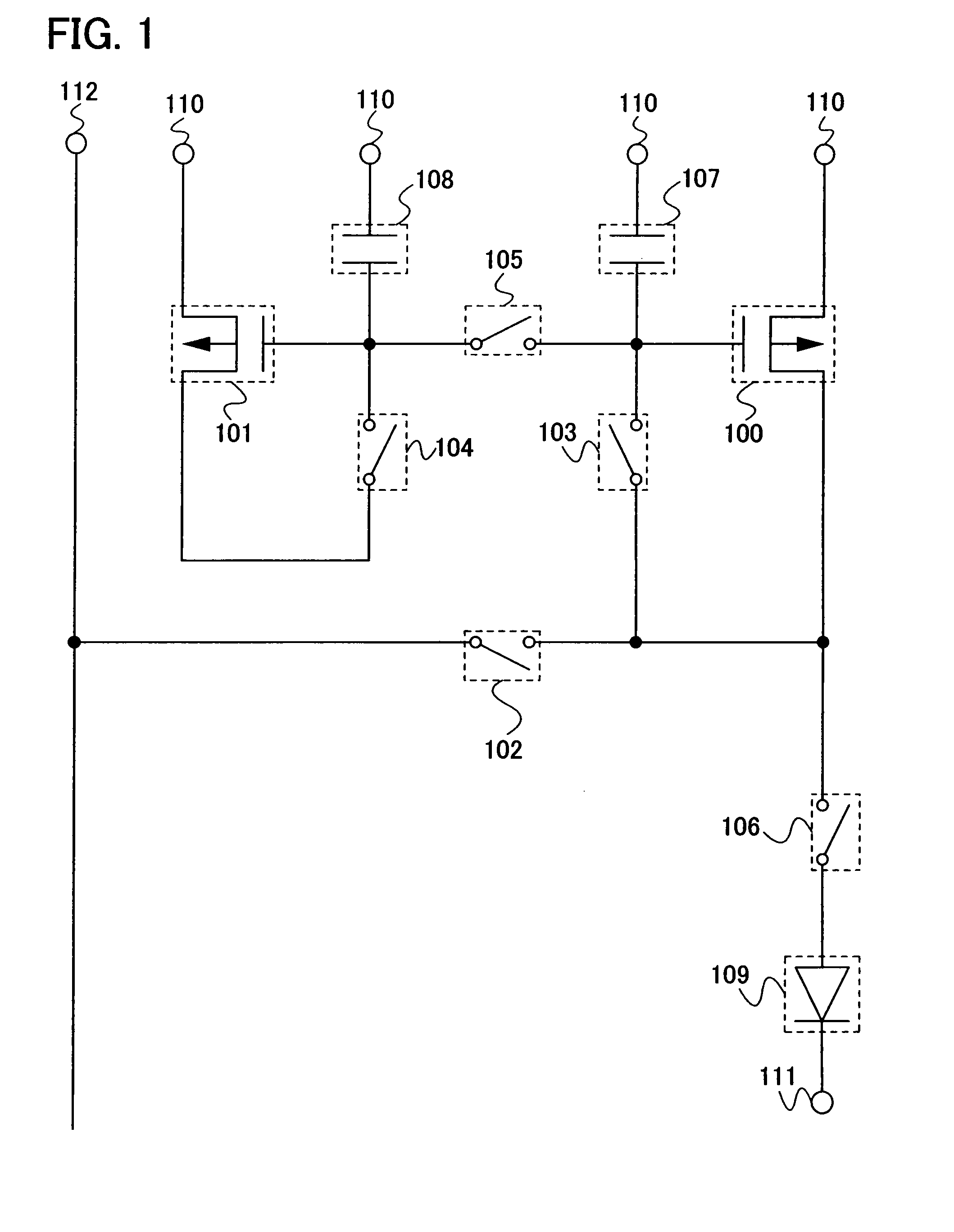
[0109]In this embodiment mode, description is made with reference to FIG. 1 of a configuration of a display device including a transistor for writing a video signal and controlling a current to be supplied to an EL element, and a transistor for obtaining a threshold voltage in order to shorten writing time per pixel.

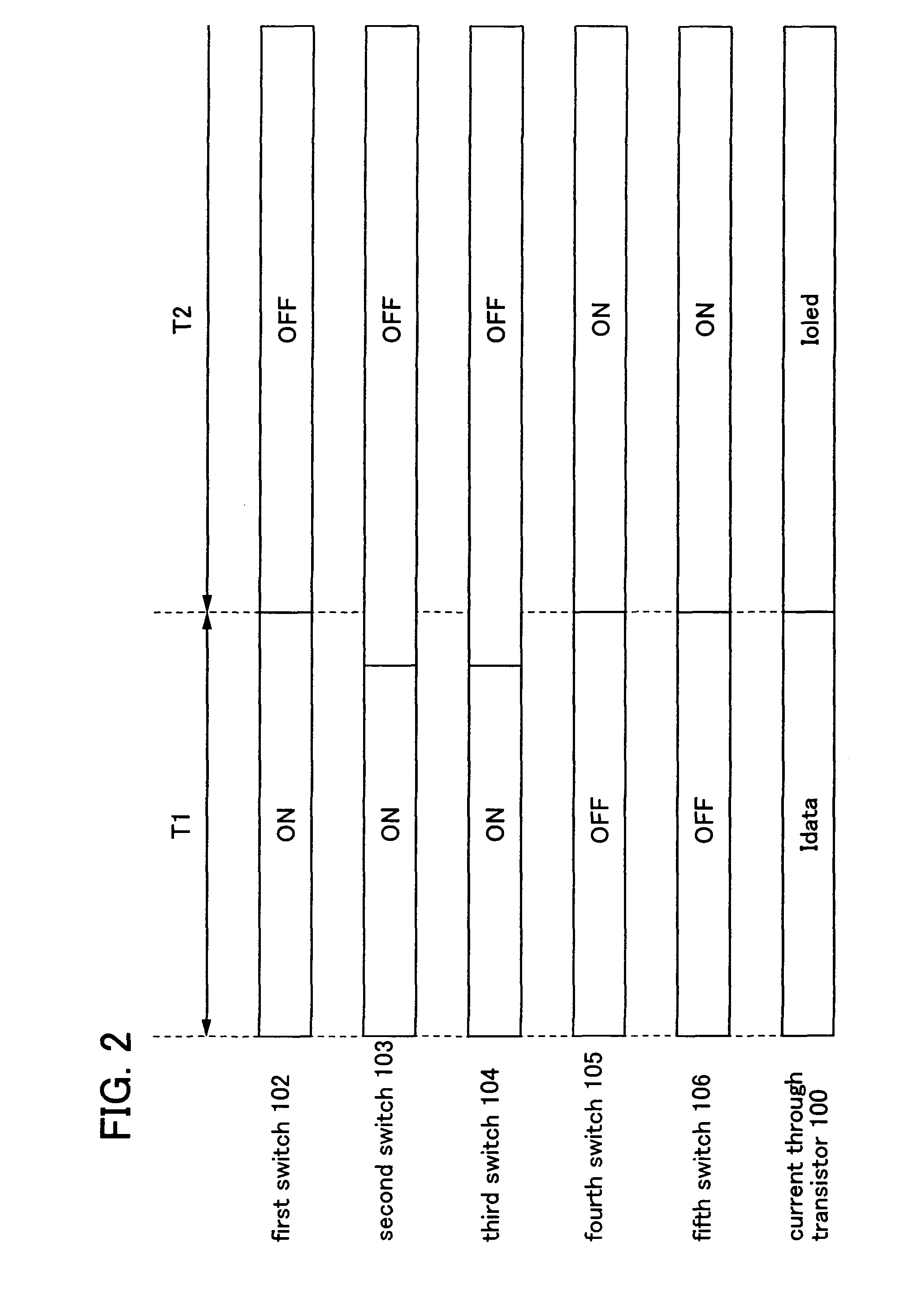
[0110]In FIG. 1, a first transistor 100 is a transistor which operates in a saturation region and controls a current value flowing through an EL element 109 by a gate-source voltage thereof. A second transistor 101 is a transistor which has similar characteristics to the first transistor 100, such as a threshold voltage and mobility and is coupled with the first transistor 100. Each of a first switch 102, a second switch 103, a third switch 104, a fourth switch 105, and a fifth switch 106 has two terminals and a control terminal. They are switching elements which control conduction (on) or non-conduction (off) between the two terminals by the control terminal. A first ca...

embodiment mode 2

[0127]In Embodiment Mode 1, a transistor can be used as a switching element. This embodiment mode describes a configuration where a p-channel transistor is used as a switching element with reference to FIG. 5.

[0128]In FIG. 5, the first transistor 100, the second transistor 101, the first capacitor 107, the second capacitor 108, the EL element 109, the power source line 110, the counter electrode 111, and the source signal line 112 are similar to those in Embodiment Mode 1. A third transistor 502, a fourth transistor 503, a fifth transistor 504, a sixth transistor 505, and a seventh transistor 506 each has a function as a switching element and operates in a linear region. The third transistor 502, the fourth transistor 503, the fifth transistor 504, the sixth transistor 505, and the seventh transistor 506 are controlled by a digital signal from a first gate signal line 512, a second gate signal line 513, a third gate signal line 514, a fourth gate signal line 515, and a fifth gate si...

embodiment mode 3

[0141]This embodiment mode describes a configuration of a display device for controlling a current supplied to an EL element by using a transistor which obtains a threshold voltage in order to prevent characteristics deterioration of a transistor due to the concentration of current to one of the transistors with reference to FIG. 7.

[0142]In FIG. 7, the first transistor 700 is a driving transistor which operates in a saturation region and controls a current value supplied to an EL element 709 by a gate-source voltage. The second transistor 701 has characteristics such as a threshold voltage and mobility similar to those of the first transistor 700 and is paired with the first transistor 700. The first switch 702, the second switch 703, the third switch 704, the fourth switch 705, and the fifth switch 706 are switching elements each having two terminals and a control terminal, which are controlled to be conductive (on) or non-conductive (off) between the two terminals by the control t...


PUM


Abstract

A first capacitor obtains a gate-source voltage of a first transistor in accordance with a programming current flowing through the first transistor, and a second capacitor obtains a threshold voltage of a second transistor. Then, the electric charges held in the first capacitor and the second capacitor are capacitively coupled. By using the voltage obtained with the capacitively coupling as a gate-source voltage of the first transistor, constant current in accordance with the programming current can be supplied to a light emitting element.

Description

BACKGROUND OF THE INVENTION[0001]1. Field of the Invention[0002]The invention relates to a display device constituted including a transistor and a driving method of the display device. In particular, the invention relates to a semiconductor device including a pixel constituted including a thin film transistor (hereinafter also called a transistor).[0003]2. Description of the Related Art[0004]An active matrix display, which is constituted by the combination of an electroluminescence element (also called an organic light emitting diode (OLED) and an EL element or a light emitting element in this specification) and a transistor, has been attracting attentions and actively researched and developed both domestically and internationally as a thin and lightweight display. This display which is also called an organic EL display (OELD) is extensively researched and developed in a practical use stage aiming for a small 2-inch display to a large display of 40-inch or larger.[0005]Luminance of ...

Claims


Application Information

Patent Timeline
Patent Type & Authority Patents(United States)
IPC IPC(8): G09G3/30H05B44/00
CPCG09G3/325H01L27/1255H01L27/1225H01L27/1251G09G2300/0819G09G2300/0852G09G2300/0861G09G2310/027G09G2310/0272H01L27/12H01L27/1214H01L27/3244H01L27/3248H01L27/3262H01L27/3265G09G2300/0408H01L27/1222H10K59/123H10K59/1213H10K59/1216H10K59/12
Inventor UMEZAKI, ATSUSHI
Owner SEMICON ENERGY LAB CO LTD
Why Eureka
Try Eureka