

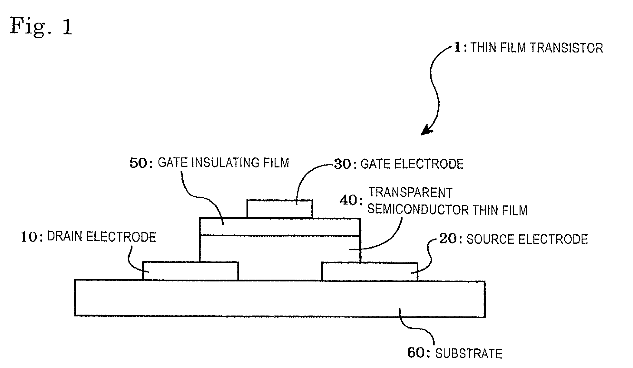
Semiconductor thin film, method for manufacturing the same, thin film transistor, and active-matrix-driven display panel
a technology of semiconductors and thin films, applied in the direction of oxide conductors, non-metal conductors, conductors, etc., can solve the problems of low switching speed, low field effect mobility, and reduced hall mobility, so as to achieve hardly erroneous operation and small leakage current
- Summary
- Abstract
- Description
- Claims
- Application Information
AI Technical Summary
Benefits of technology
Problems solved by technology
Method used
Image

Examples
examples
[0094]By using concrete examples, the present invention will be described in more detail below.
first example
(1) Manufacture and Evaluation of Sputtering Target
1. Manufacture of Target
[0095]As materials, indium oxide having an average particle diameter of 3.4 μm and zinc oxide having an average particle diameter of 0.6 μm were mixed so that the atom ratio [In / (In+Zn)] becomes 0.28 and the atom ratio [Zn / (In+Zn)] becomes 0.72. The mixture was supplied to a wet ball mill and mixed and ground for 72 hours to obtain material fine powders.
[0096]The obtained material fine powders were granulated and, after that, pressed to a shape having a diameter of 10 cm and a thickness of 5 mm. The resultant was put in a firing furnace and sintered under conditions of 1,400° C. and 48 hours under pressure of oxygen gas, thereby obtaining a sintered body (target). The rate of temperature rise was 3° C. / minute.
2. Evaluation of Target
[0097]The density and a bulk resistance value of the obtained target were measured. As a result, theoretical relative density was 99% and the bulk resistance value measured by a fo...
PUM
| Property | Measurement | Unit |
|---|---|---|
| energy band gap | aaaaa | aaaaa |
| work function | aaaaa | aaaaa |
| transmittance | aaaaa | aaaaa |
Abstract
Description
Claims
Application Information