Semiconductor thin film and method for manufacturing same, and thin film transistor

a semiconductor and thin film technology, applied in the direction of transistors, tin compounds, chemistry apparatus and processes, etc., can solve the problems of semiconductors not being able to follow high-speed display of moving pictures, crystalline silicon thin films cannot be formed, and the semiconductor cannot. achieve the effect of hardly erroneous operation and small leakage curren

Active Publication Date: 2009-10-29
IDEMITSU KOSAN CO LTD
View PDF4 Cites 69 Cited by
  • Summary
  • Abstract
  • Description
  • Claims
  • Application Information

AI Technical Summary

Benefits of technology

[0035]As described above, the present invention can provide a semiconductor thin film as a component of an excellent field effect transistor which can be formed on a glass substrate, a resin substrate, or the like in a wide temperature range, which is stable to a visible ray and hardly erroneously operates, and in which leak current is small. The semiconductor thin film of the present invention can be formed at a relatively low temperature. Consequently, by forming the semiconductor thin film on a resin substrate, a flexible thin film transistor or the like can be also provided.

Problems solved by technology

However, at the time of crystallizing a crystalline silicon thin film, a high temperature such as 800° C. or higher is necessary, so that it is difficult to form the crystalline silicon thin film on a glass substrate or an organic substrate.
There are consequently problems such that a crystalline silicon thin film can be formed only on an expensive substrate having high heat resistance such as silicon wafer, quartz, or the like, and enormous energy and a number of processes are required for manufacture.
Therefore, when the amorphous silicon semiconductor is used as a switching device for driving a display, there is the case that the semiconductor cannot follow high speed display of a moving picture.
There is the possibility such that a leak current is generated, and an erroneous operation is performed.
A problem occurs such that the characteristics of the switching device deteriorate.
In this case as well, a problem occurs such that parasitic capacitance is generated.

Method used


Image

  • Semiconductor thin film and method for manufacturing same, and thin film transistor
  • Semiconductor thin film and method for manufacturing same, and thin film transistor

Examples


first embodiment

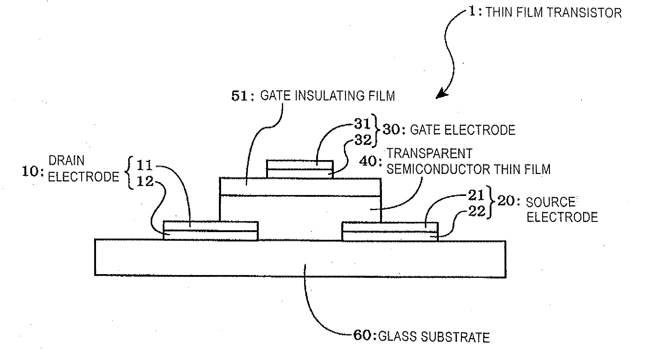
[0041]A first embodiment of a thin film transistor according to the present invention will be described.

[0042]FIG. 1 is an explanatory diagram showing outline of the first embodiment of the thin film transistor according to the present invention.

[0043]In the example of the diagram, in a thin film transistor 1 as a field effect transistor, a drain electrode 10 and a source electrode 20 are formed so as to be apart from each other on a glass substrate 60, a transparent semiconductor thin film 40 is formed so as to be in contact with at least a part of each of the drain electrode 10 and the source electrode 20, and a gate insulating film 50 and a gate electrode 30 are formed in order on the transparent semiconductor thin film 40. In such a manner, the thin film transistor 1 is constructed as the thin film transistor 1 of a top gate type.

[0044]In the embodiment, as the substrate 60, any substrate which is generally used for a thin film transistor of this kind such as an Si wafer substra...

second embodiment

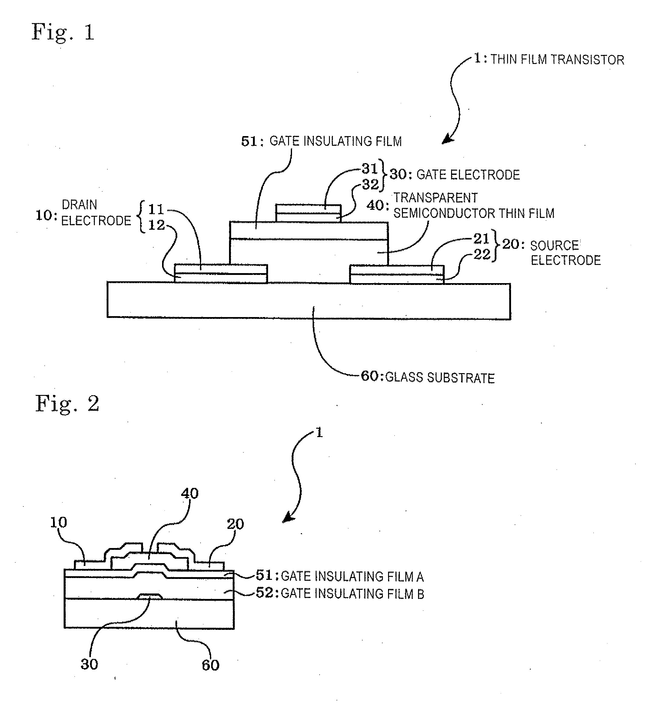
[0095]A second embodiment of the thin film transistor of the present invention will now be described.

[0096]FIG. 2 is an explanatory diagram showing outline of the second embodiment of the thin film transistor according to the present invention.

[0097]In the example of the diagram, in the thin film transistor 1, a gate insulating film B 52 and a gate insulating film A 51 are stacked in this order on the gate electrode 30 formed on the glass substrate 60 and, further, the transparent semiconductor thin film 40 is formed on the gate insulating film A 51. On both side parts of the transparent semiconductor thin film 40, the source electrode 20 and the drain electrode 10 are formed. In such a manner, the thin film transistor 1 of the bottom gate type is constructed.

[0098]In the foregoing first embodiment, the thin film transistor of the top gate type has been described. It can be a thin film transistor of the bottom gate type as in the second embodiment.

[0099]In the thin film transistor o...

examples

[0101]By using concrete examples, the present invention will be described in more detail below.


PUM

PropertyMeasurementUnit
energy band gapaaaaaaaaaa
transmittanceaaaaaaaaaa
wavelengthaaaaaaaaaa

Abstract

The present invention provides a semiconductor thin film which can be manufactured at a relatively low temperature even on a flexible resin substrate. As a semiconductor thin film having a low carrier concentration, a high Hall mobility and a large energy band gap, an amorphous film containing zinc oxide and tin oxide is formed to obtain a carrier density of 10+17 cm−3 or less, a Hall mobility of 2 cm2/V·sec or higher, and an energy band gap of 2.4 eV or more. Then, the amorphous film is oxidized to form a transparent semiconductor thin film 40.

Description

TECHNICAL FIELD[0001]The present invention relates to a semiconductor thin film made of an amorphous film containing zinc oxide and tin oxide, a method for manufacturing the same, and a thin film transistor using such a semiconductor thin film.BACKGROUND ART[0002]A field effect transistor is widely used as a unit electronic device of a semiconductor memory integrated circuit, a high-frequency signal amplification device, a liquid crystal drive device, or the like and is an electronic device which is most practically used at present.[0003]Among the devices, with remarkable development of displays in recent years, a thin film transistor (TFT) is often used as a switching device for driving a display by applying a drive voltage to a display device in not only a liquid crystal display (LCD) but also various displays such as an electroluminescence display (EL) and a field emission display (FED).[0004]As the material of the thin film transistor, a silicon semiconductor compound is used mo...

Claims


Application Information

Patent Timeline
Patent Type & Authority Applications(United States)
IPC IPC(8): H01L29/786H01L29/26H01L21/336
CPCC01G19/00H01L29/7869C01P2006/40
Inventor YANO, KOKIINOUE, KAZUYOSHITANAKA, NOBUOTANAKA, TOKIE
Owner IDEMITSU KOSAN CO LTD
Why Eureka
Try Eureka