Semiconductor device and manufacturing method thereof

a semiconductor and semiconductor technology, applied in the direction of semiconductor devices, electrical devices, transistors, etc., can solve the problems of not lowering current amplification efficiency, the thickness of the gate electrode, and the above-described conventional techniques are not suitable for integration with logic circuits, so as to achieve the effect of increasing short-circuit ruggedness

Inactive Publication Date: 2011-08-16
FUJI ELECTRIC CO LTD
View PDF51 Cites 11 Cited by
  • Summary
  • Abstract
  • Description
  • Claims
  • Application Information

AI Technical Summary

Benefits of technology

[0048]Between the low-resistivity region forming step and the gate insulating film forming step, annealing may be performed at 900° C. to 960° C. for 20 to 40 minutes in a nitrogen atmosphere to repair crystal lattice disorder that may occur during the forming the low-resistivity region and preventing excessive diffusion from occurring in the low resistivity region.
[0049]According to the invention, the impurity concentration profile of the low-resistivity region has two local maxima. Therefore, the width of that portion of the low-resistivity region which is located under the gate electrode can be set at a desired value, which makes it possible to suppress a punchthrough occurring in the channel.
[0051]Consequently, the semiconductor devices and their manufacturing methods according to the invention provide an advantage that their short-circuit ruggedness can be increased.

Problems solved by technology

This raises a problem that the gate electrode should be so thick that ions do not pass through it at the time of the ion implantation.
Therefore, there is a problem that the above-described conventional techniques are not suitable for integration with logic circuits.
However, there is a problem that since a second npn bipolar transistor which is composed of the n+ emitter region 105, the p-type body region 104, and the n− drift region 103 does not include the p+ low-resistivity region 141, its current amplification efficiency is not lowered and hence is prone to a latch-up phenomenon.
This results in a problem that the entire device becomes prone to the latch-up phenomenon.
And there is another problem that the impurity concentration of the p+ low-resistivity region is limited so as not to lower the breakdown voltage of the pn junction formed by the n− drift region and the p-type body region.
This means a problem that the width of the p+ low-resistivity region cannot be made greater than that of the lateral extension of the diffusion.

Method used


Image

  • Semiconductor device and manufacturing method thereof
  • Semiconductor device and manufacturing method thereof
  • Semiconductor device and manufacturing method thereof

Examples


embodiment 1

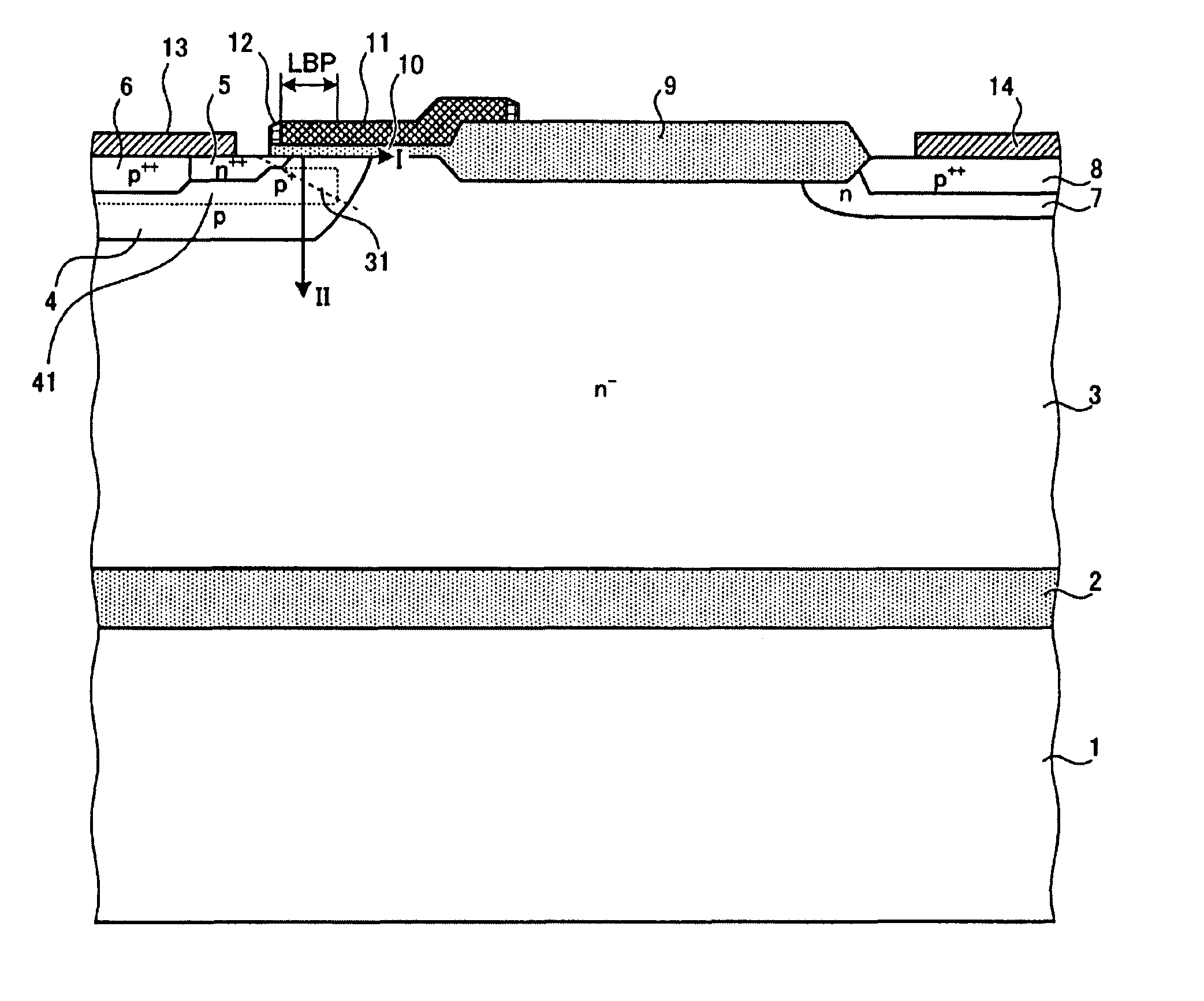
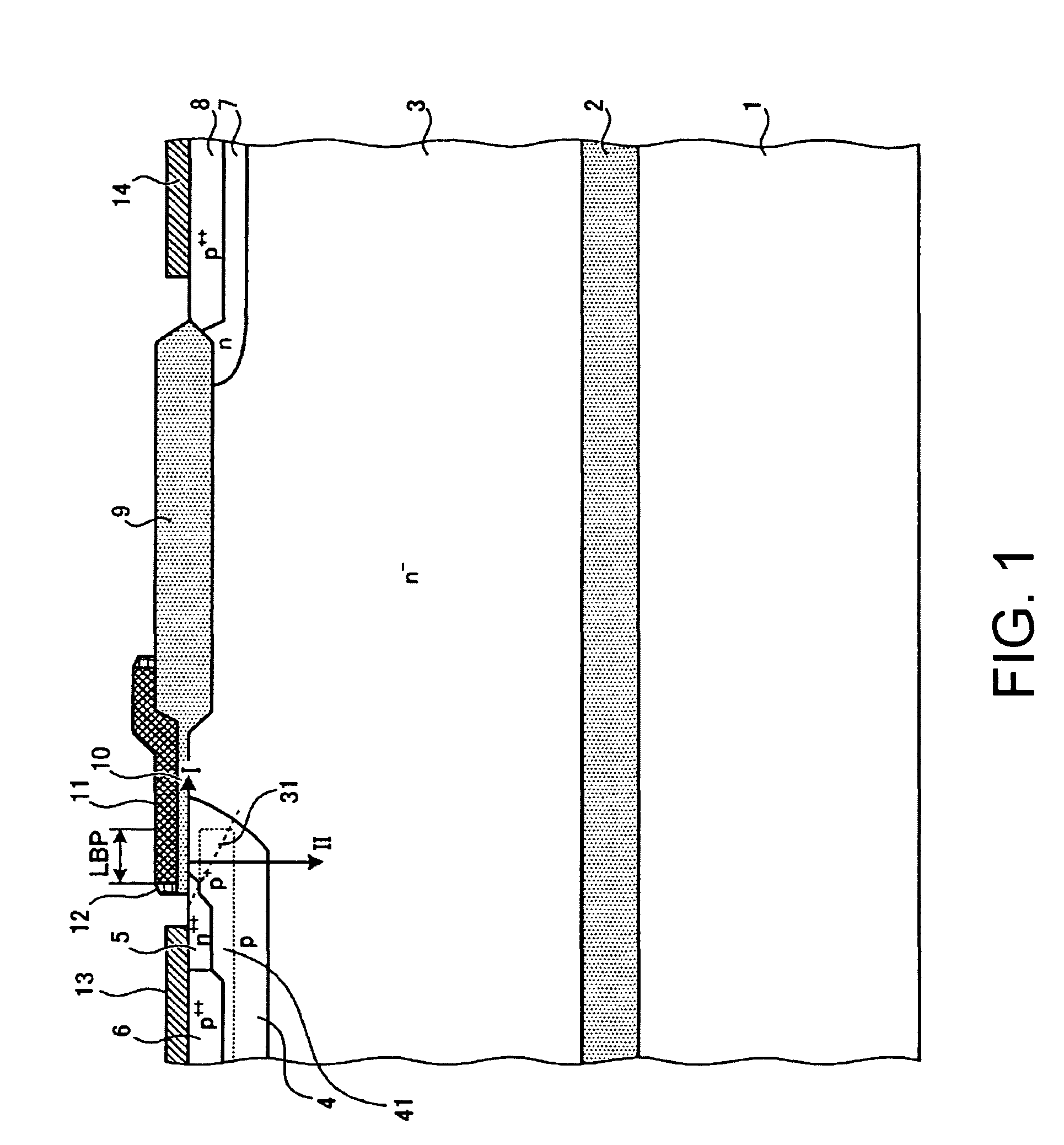
[0067]FIG. 1 shows the configuration of a semiconductor device according to the first embodiment. The semiconductor device shown in FIG. 1 is manufactured by using an SOI substrate. The SOI substrate is configured in such a manner that a buried oxide (BOX) region 2 and an n drift region 3 as a first semiconductor region are laid in this order on a support substrate 1. The BOX region 2 insulates the n− drift region 3 and the support substrate 1 from each other. A p-type body region 4 as a second semiconductor region is formed as a partial surface region of the n− drift region 3. An n++ emitter region 5 as a third semiconductor region is formed as a partial surface region of the p-type body region 4. The n++ emitter region 5 is lower in resistivity than the n drift region 3. A p++ contact region 6 is formed as a partial surface region of the p-type body region 4 so as to be in contact with the n++ emitter region 5. The p++ contact region 6 is lower in resistivity than the p-type body ...

embodiment 2

[0104]FIG. 19 shows the configuration of a semiconductor device according to the second embodiment. As shown in FIG. 19, the semiconductor device according to the second embodiment is different from the semiconductor device according to the first embodiment in that the n-type buffer region 7, the p+ collector region 8, and the collector electrode 14 are formed adjacent to the surface of the n− drift region 3 which is opposite to its surface that is formed with the p-type body region 4. As a result, the semiconductor device according to the second embodiment is a vertical IGBT structure. The semiconductor device having the vertical IGBT structure can be manufactured by using a p+ substrate to serve as the p+ collector region 8. The n-type buffer region 7 is formed on one major surface of the p+ substrate and the n− drift region 3 is formed on the surface of the n-type buffer region 7. The collector electrode 14 is formed on the other major surface of the p+ substrate. The other part ...

embodiment 3

[0106]FIG. 20 shows the configuration of a semiconductor device according to the third embodiment. As shown in FIG. 20, the semiconductor device according to the third embodiment is different from the semiconductor device according to the first embodiment in that the first n+ emitter region 5a and a second n+ emitter region 5b are formed in the p-type body region 4 and disposed away from each other. The p++ contact region 6 is formed between the first n+ emitter region 5a and the second n+ emitter region 5b so as to be in contact with them. The p+ low-resistivity region 41 is formed to surround the interfaces between the p-type body region 4 and the first n+ emitter region 5a, the p++ contact region 6, and the second n+ emitter region 5b.

[0107]The emitter electrode 13 is formed so as to be in contact with the first n+ emitter region 5a, the p+ contact region 6, and the second n+ emitter region 5b and short-circuits them. The first gate insulating film 10a which is in contact with t...


PUM


Abstract

A p-type body region and an n-type buffer region are formed on an n− drift region. An n++ emitter region and a p++ contact region are formed on the p-type body region in contact with each other. A p++ collector region is formed on the n-type buffer region. An insulating film is formed on the n− drift region, and a gate insulating film is formed on the n++ emitter region, the p-type body region, and the n drift region. A gate electrode is formed on the insulating film and the gate insulating film. A p+ low-resistivity region is formed in the p-type body region and surrounding the interface between the n++ emitter region and between the p-type body region and the p++ contact region. The p-type body region has two local maxima of an impurity concentration profile at the interface between the body region and the gate insulating film.

Description

CROSS-REFERENCE TO RELATED APPLICATION[0001]This application claims the benefit of priority of Japanese patent application number 2008-005013, filed on Jan. 11, 2008, the entire disclosure of which is incorporated herein by reference.BACKGROUND OF THE INVENTION[0002]1. Field of the Invention[0003]The invention relates to an insulated-gate semiconductor device and a manufacturing method thereof.[0004]2. Description of the Related Art[0005]Power devices manufactured by using SOI (silicon on insulator) substrates are known. Thick film SOI substrates are used for vehicular engine control and in drive circuits of plasma displays because they make it possible to isolate devices from each other easily by forming trenches and possible to suppress variations in manufacturing because they have a thick silicon layer. Example power devices that are manufactured by using SOI substrates include IGBTs (insulated-gate bipolar transistors) and MOSFETs (metal oxide semiconductor field-effect transist...

Claims


Application Information

Patent Timeline
Patent Type & Authority Patents(United States)
IPC IPC(8): H01L29/66
CPCH01L29/1095H01L29/7394H01L29/7816H01L29/7824H01L29/086H01L29/0878H01L29/42368
Inventor LU, HONG-FEITOMONORI, MIZUSHIMA
Owner FUJI ELECTRIC CO LTD
Why Eureka
Try Eureka