Epitaxial wafer for semiconductor light-emitting devices, and semiconductor light-emitting device

a light-emitting device and semiconductor technology, applied in the direction of semiconductor devices, basic electric elements, electrical appliances, etc., can solve the problems of deterioration of device characteristics and reliability, increase of threshold current and operating current, and impaired crystal quality of active layer, etc., to achieve excellent high-power and high-temperature characteristics, no deterioration of luminescent characteristics, and less diffusion

Inactive Publication Date: 2006-01-05
HITACHI CABLE
View PDF2 Cites 11 Cited by
  • Summary
  • Abstract
  • Description
  • Claims
  • Application Information

AI Technical Summary

Benefits of technology

[0094] According to the present invention, since the p-type cap layer comprising GaAs has an at-least-two-layered structure where the layer close to the n-type substrate and active layer is the Mg-doped p-type layer comprising GaAs and the other layer is the Zn-doped p-type layer comprising GaAs, and the Mg-doped p-type cap layer serves as a zinc diffusion suppression layer for suppressing diffusion of Zn in the other Zn-doped p-type cap layer, almost no diffusion of Zn in the p-type cap layer to the active layer side relative to the Mg-doped p-type cap layer is caused. In other words, since diffusion of Zn in the p-type cap layer into the cladding layer and especially into the active layer can very effectively be suppressed, no deterioration is caused in luminescent characteristics of the active layer and the life of the device. This results in less diffusion which therefore allows sufficiently taking advantage of use of Mg which can be doped to a high concentration in the p-type cladding layer, etc., and can provide an epitaxial wafer for semiconductor light-emitting devices suitable for the fabrication of light-emitting devices such as red semiconductor lasers, etc. which are excellent in high-power and high-temperature characteristics.

Problems solved by technology

However, doping Zn to a high concentration would cause Zn to diffuse into an active layer during epitaxial growth, which would result in the problem of deterioration of device characteristics and reliability.
To achieve stable high-power and high-temperature operation, it is desirable that the carrier concentration of the p-type cladding layer is made as high as possible, but when Zn is used as the p-type dopant as in the conventional art, as the carrier concentration of the p-type cladding layer is made higher, Zn is caused to diffuse into the active layer, which results in a larger photoluminescence spectrum full width at half maximum (hereinafter, PL FWHM) of the active layer, and impaired crystal quality of the active layer, which becomes the cause of an increase in threshold current and operating current, and a reduction in reliability.
As a problem, however, it has been found out that doping the carrier concentration of the p-type cladding layer to a higher concentration than 1×1018 cm−3 makes mutual diffusion of Zn and Mg remarkable, which results in the phenomenon of Zn of the p-type contact layer diffusing into the p-type cladding layer and active layer which are not at all doped with Zn.
Therefore, there is the problem that further doping to a higher concentration than 1×1018 cm−3 results in a larger PL FWHM of the active layer, as in the case of use of Zn only as the p-type dopant.
In other words, in the prior art, when Zn which tends to diffuse is used as the p-type dopant of the p-type GaAs cap layer formed in the top layer, there is the problem that Zn doped into this p-type GaAs cap layer is caused to diffuse through the underlying p-type cladding layer into the active layer during its growth, which results in a deterioration in luminescent characteristics of the active layer.
As explained as the above prior application, in the case of use of Mg as the p-type dopant of the p-type cladding layer, particularly this Zn diffusion is remarkable, and in addition, diffusion of Mg which should originally be relatively difficult to diffuse is facilitated, which results in the significant problem of deterioration in luminescent characteristics of the active layer and the life of the device.

Method used


Image

  • Epitaxial wafer for semiconductor light-emitting devices, and semiconductor light-emitting device
  • Epitaxial wafer for semiconductor light-emitting devices, and semiconductor light-emitting device
  • Epitaxial wafer for semiconductor light-emitting devices, and semiconductor light-emitting device

Examples


embodiment 1

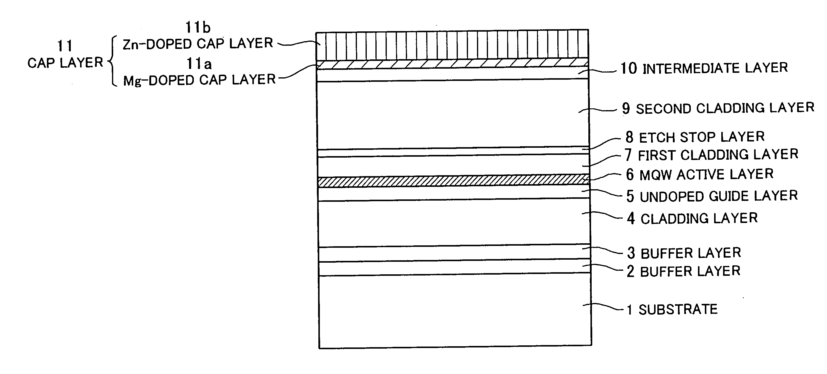
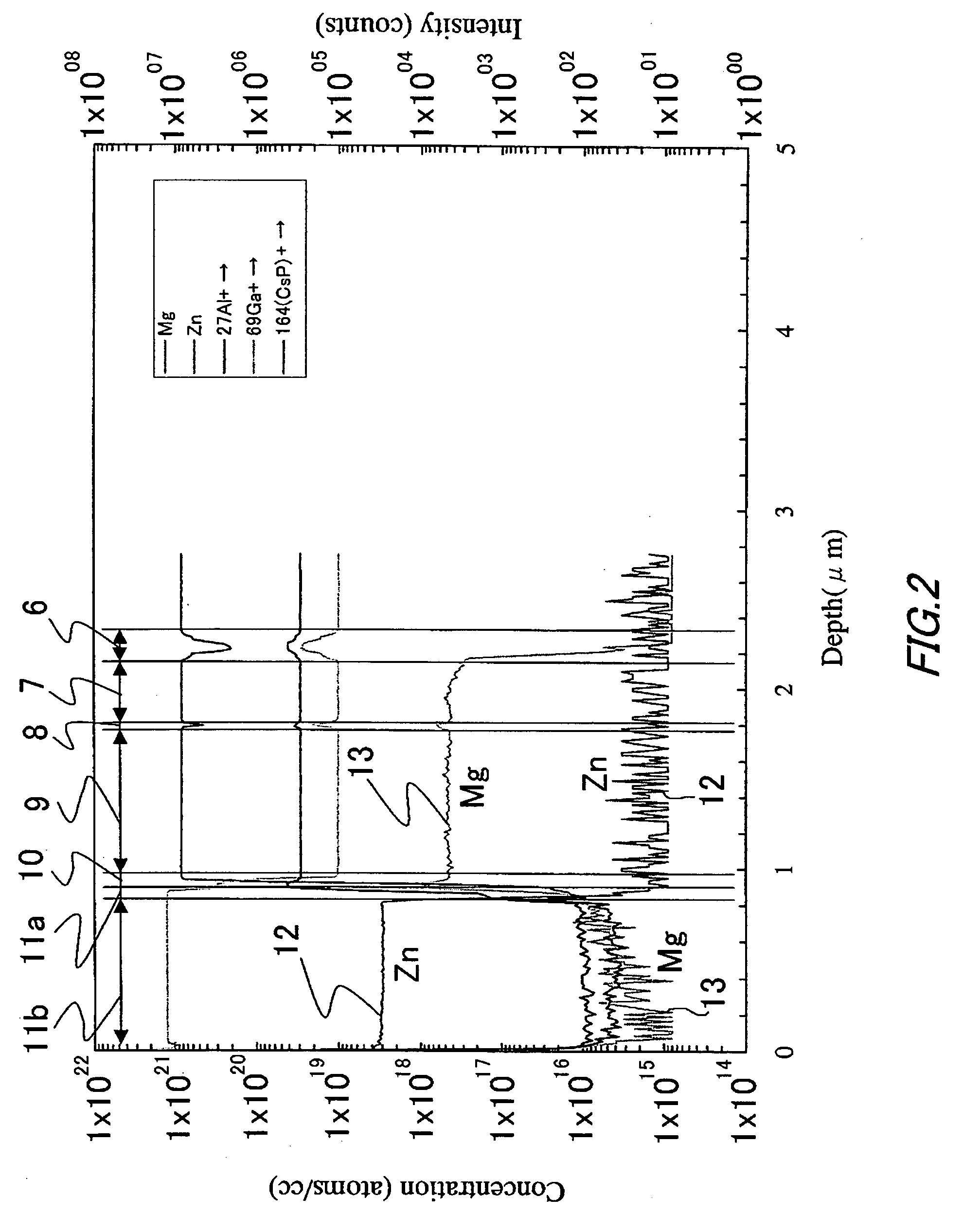
[0106] As shown in FIG. 1, on an n-type substrate 1 made of GaAs are sequentially epitaxially grown an n-type buffer layer 2 made of GaAs, a lattice-matched n-type buffer layer 3 made of GaInP, and a lattice-matched n-type cladding layer 4 made of (Al0.7Ga0.3) 0.5In0.5P, on which are sequentially grown an undoped guide layer 5 made of (Al0.5Ga0.5)0.5In0.5P, a multi-quantum well (MQW) active layer 6 constituted by a barrier layer and a strained GaInP well layer, a Mg-doped p-type first cladding layer 7 made of (Al0.7Ga0.3) 0.5In0.5P, a p-type etch stop layer 8 made of GaInP, a Mg-doped p-type second cladding layer 9 made of (Al0.7Ga0.3)0.5In0.5P, and a Mg-doped p-type intermediate layer 10 made of GaInP.

[0107] And on the top portion are sequentially grown a Mg-doped p-type cap layer 11a made of GaAs serving as the zinc diffusion suppression layer of the invention, and a Zn-doped p-type cap layer 11b made of GaAs. Here, the Mg-doped p-type cap layer 11a on the Mg-doped p-type second ...

embodiment 2

[0111] For the zinc diffusion suppression layer (Mg-doped p-type cap layer 11a) of the invention, the amount of Mg doped can be freely set to some degree. Accordingly, as another embodiment, by setting the carrier concentration of the Mg-doped p-type cap layer 11a that is the zinc diffusion suppression layer to 4×1018 cm−3, and likewise the carrier concentration of the Zn-doped p-type cap layer 11b to 4×1018 cm−3, similar effects can be exhibited.

embodiment 3

[0112] As shown in FIG. 3, on an n-type substrate 21 made of GaAs are sequentially epitaxially grown an n-type buffer layer 22 made of GaAs, an n-type DBR (distributed Bragg reflector) layer 23 made of a thin-film multi-layer structure of Al0.5Ga0.5As and AlAs, and an n-type cladding layer 24 made of (Al0.7Ga0.3)0.5In0.5P, on which are sequentially grown a multi-quantum well (MQW) active layer 25 constituted by a barrier layer and a strained GaInP well layer, a Mg-doped p-type cladding layer 26 made of (Al0.7Ga0.3)0.5In0.5P, and a p-type current diffusion layer 27 made of GaP.

[0113] And on the top portion are sequentially grown a Mg-doped p-type cap layer 28a made of GaAs serving as the zinc diffusion suppression layer of the invention, and a Zn-doped p-type cap layer 28b made of GaAs. Here, the Mg-doped p-type cap layer 28a on the Mg-doped p-type cladding layer 26 side is 70 nm in thickness and 1×1018 cm−3 in carrier concentration, and the Zn-doped p-type cap layer 28b on the uppe...


PUM


Abstract

An epitaxial wafer for semiconductor light-emitting devices has an n-type substrate, on which are sequentially formed an n-type cladding layer, an active layer, a p-type cladding layer having Mg as a p-type dopant, and a p-type cap layer. The p-type cap layer has at least two Mg-doped and Zn-doped layers that are formed sequentially from the substrate side.

Description

[0001] The present application is based on Japanese patent application Nos. 2004-165187 and 2005-037363, the entire contents of which are incorporated herein by reference. BACKGROUND OF THE INVENTION [0002] 1. Field of the Invention [0003] The present invention relates to an epitaxial wafer for semiconductor light-emitting devices (light-emitting diodes, semiconductor lasers), and particularly, to an epitaxial wafer for semiconductor light-emitting devices suitable for aluminum gallium indium phosphorus (AlGaInP) series light-emitting devices using magnesium (Mg) as a p-type dopant, and a semiconductor light-emitting device fabricated using the same. [0004] 2. Description of the Related Art [0005] Generally, conventional AlGaInP series crystal growth for semiconductor light-emitting devices using metal organic vapor phase epitaxy (MOVPE) uses silicon (Si) and selenium (Se) as n-type dopants, and zinc (Zn) and Mg as p-type dopants. In epitaxial wafers for semiconductor laser (LD) app...

Claims


Application Information

Patent Timeline
Patent Type & Authority Applications(United States)
IPC IPC(8): H01L33/00H01L33/06H01L33/30
CPCH01L33/30H01L33/14
Inventor SUZUKI, RYOJIOHISHI, AKIO
Owner HITACHI CABLE
Why Eureka
Try Eureka