Circuit distribution to multiple integrated circuits

a technology of integrated circuits and circuits, applied in the field of electronic packages, can solve the problems of increasing increasing signal delay and parasitics in conductors, and becoming more and more difficult to achieve the reduction of minimum feature size in fpgas, so as to reduce the number of layers of metallization, reduce the density of logic elements, and achieve the effect of minimum or zero performance penalty

Active Publication Date: 2011-08-16
ALTERA CORP
View PDF6 Cites 4 Cited by
  • Summary
  • Abstract
  • Description
  • Claims
  • Application Information

AI Technical Summary

Benefits of technology

[0008]I have devised a semiconductor system in a package that separates the circuits of a device, such as an FPGA, that otherwise would be implemented on a single integrated circuit chip into at least two chips that are stacked one on top of the other. In one embodiment, the logic elements of an FPGA are formed on a first semiconductor substrate and the other circuits of the FPGA are formed on either the first substrate or a second semiconductor substrate that is in mechanical and electrical connection with the first substrate. As a result, the size of each of the substrates can be reduced relative to the size of a conventional FPGA, thereby reducing the length of the global horizontal and vertical buses that traverse the substrate and reducing delays and parasitics.
[0012]In addition to the performance benefits achievable with the invention, it should also be possible to reduce the number of layers of metallization on the first semiconductor substrate containing the logic elements. It should also be possible to increase the density of logic elements in the first semiconductor substrate with minimum or zero penalty on performance.

Problems solved by technology

In recent years, however, it has become more and more difficult to achieve desired reductions in minimum feature size in FPGAs for a variety of reasons.
Some of these difficulties relate to increased signal delay and parasitics in conductors.
It has been observed that such delays and parasitics increase as the width of the conductor decreases.
At a technology node such as the 45 nanometer (nm.) node, such delays and parasitics can become unacceptable even in copper conductors when such conductors have the length of the global horizontal or vertical interconnect circuitry used in a conventional FPGA integrated circuit.

Method used


Image

  • Circuit distribution to multiple integrated circuits
  • Circuit distribution to multiple integrated circuits
  • Circuit distribution to multiple integrated circuits

Examples


Embodiment Construction

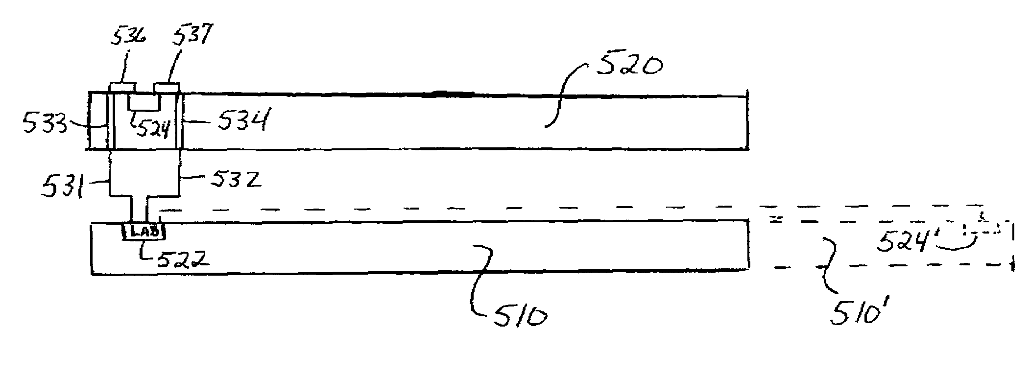
[0020]FIG. 4 depicts a system in a package in a first embodiment of the invention. System 400 comprises a first semiconductor substrate 410 and a second semiconductor substrate 420 that are stacked on one another. Substrates 410 and 420 are mechanically and electrically connected together by an array of solder balls or solder bumps (not shown). Substrate 410 is connected by solder bumps, wire bonds (not shown) or equivalent to the individual leads of a conventional lead frame (not shown). A conventional package 450 encloses substrates 410, 420, solder bumps and wire bonds.

[0021]Also shown in FIG. 4 for comparison purposes is the outline in dashes of a conventional FPGA integrated circuit 460. Assuming that the circuits of the conventional FPGA can be distributed approximately equally between the two substrates, the lateral dimensions of the FPGA can be reduced by almost 30% in each direction.

[0022]In accordance with the invention, logic elements are formed on the first semiconductor...


PUM


Abstract

A semiconductor system in a package separates those circuits in a field programmable gate array (FPGA) into two substrates. In particular, the logic elements are formed in a first semiconductor substrate and certain non-logic elements are formed in a second semiconductor substrate that is in mechanical and electrical connection with the first substrate. The two substrates are enclosed in a suitable protective package and electrical connections are provided between one or both substrates and the exterior. The non-logic elements formed in the second substrate are located in circuits that would have a signal propagation delay in a conventional FPGA that is more than approximately twice the interconnect delay between the two substrates.

Description

CROSS-REFERENCE TO RELATED APPLICATION[0001]This application claims the benefit of provisional application No. 60 / 878,911, filed Jan. 5, 2007 which is hereby incorporated by reference in its entirety.BACKGROUND[0002]The present invention relates generally to an electronic package and a method for making it and, in particular, to an electronic package in which multiple integrated circuits are stacked one above another. A particular application for this package is in the implementation of field programmable gate arrays (FPGA) and the invention will be described in that context.BACKGROUND OF THE INVENTION[0003]A FPGA is a programmable logic device containing a large number of small programmable logic elements, a number of input / output (I / O) terminals, and a method of specifying electrical connections between the logic elements through a distributed array of programmable switches. The programming of the logic elements and the switches is typically specified by configuration bits stored ...

Claims


Application Information

Patent Timeline
Patent Type & Authority Patents(United States)
IPC IPC(8): H05K7/00
CPCH01L23/481H01L24/16H01L25/18H01L2224/13099H01L2224/32145H01L2924/01029H01L2924/01082H01L2924/14H01L2924/01006H01L2924/01023H01L2924/01033H01L2924/014H01L2225/06513H01L2225/06541H01L2225/06565
Inventor PATEL, RAKESH H.
Owner ALTERA CORP
Why Eureka
Try Eureka