Unipolar semiconductor photodetector with suppressed dark current and method for producing the same

a photodetector and semiconductor technology, applied in the field of photodiodes, can solve the problems of cumbersome and expensive means for cooling and maintaining such a low temperature in photodiodes, reducing noise to a limited value, and limiting the signal-to-noise ratio which can be obtained from photodiodes (and many other electronic components)

Active Publication Date: 2011-08-23
SEMICON DEVICES AN ELBIT SYSTEMSRAFAEL PARTNERSHIP IL
View PDF9 Cites 19 Cited by
  • Summary
  • Abstract
  • Description
  • Claims
  • Application Information

AI Technical Summary

Problems solved by technology

It is well known in the art that the signal-to-noise ratio which can be obtained from photodiodes (and from many other electronic components) is limited by the level of the “thermal noise”, which in turn is related to the temperature of the component.
The signal-to-noise ratio in photodiodes is conventionally improved by cooling the component, in many cases down to very low temperatures close to 0° K. The means for cooling and maintaining such a low temperature in photodiodes, however, are cumbersome and expensive, and in any case can reduce the noise down to a limited value.
However, there are not known many of such efforts for reducing the G-R current.
Until recently, the prior art has failed to specifically address the issue of suppressing the G-R contribution to the current by a suitable hetero-junction design.

Method used


Image

  • Unipolar semiconductor photodetector with suppressed dark current and method for producing the same
  • Unipolar semiconductor photodetector with suppressed dark current and method for producing the same
  • Unipolar semiconductor photodetector with suppressed dark current and method for producing the same

Examples


embodiment 1

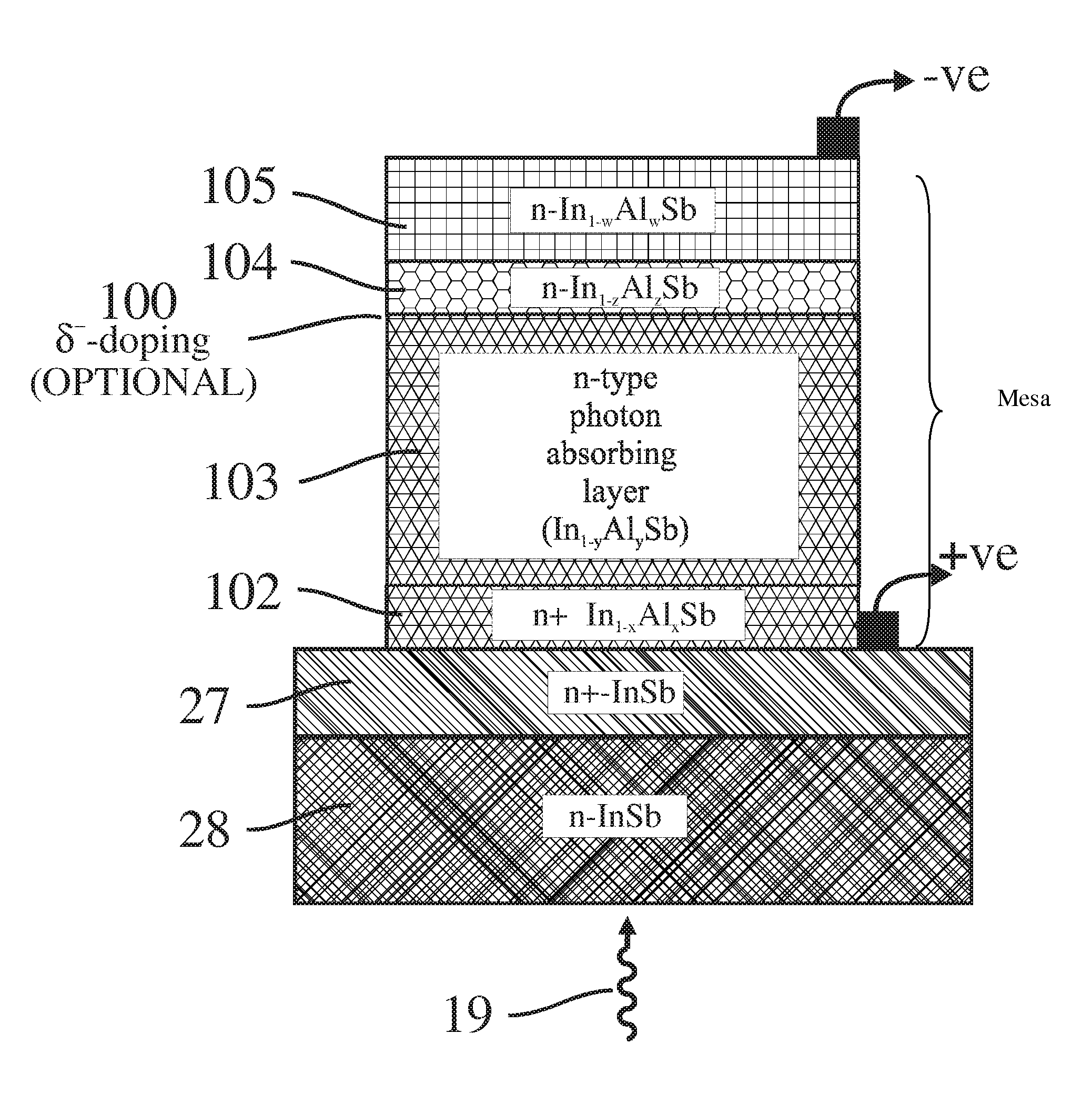
[0103]A band diagram of a first embodiment of the invention is shown in FIG. 4a. Examples of the structure of said first embodiment are shown in FIGS. 4b and 4c. In the first embodiment, band bending is allowed in the barrier layer 24 and a short distance into the contact layer 75. Band bending in the contact layer 75 is usually due to electron accumulation close to the barrier (210A in FIG. 3a). The bands in the photon absorbing layer 23 are flat at the maximum operating bias but a small accumulation layer of electrons (210 in FIG. 3a) forms close to the barrier layer at lower bias, as shown in FIG. 4a.

[0104]The n-type photon-absorbing layer 23 is made of InAsSb alloy. The doping is typically in the range of n16 cm−3 and the thickness is typically in the range 1-10 μm.

[0105]The use of InAsSb enables operation in the MWIR atmospheric transmission window (3-5 μm).

[0106]The contact layer 75 is made of n-type InAsSb with typical values of doping in the range 5×101416 cm−3 and thicknes...

embodiment 2

[0110]A band diagram of a second embodiment of the invention is shown in FIG. 5a. An example of the structure of said second embodiment is shown in FIG. 5b. The n-type photon-absorbing layer 23 is made of InAsSb alloy. The doping is typically in the range n16 cm−3, and the thickness of the photon-absorbing layer 23 is typically in the range 1-10 μm. The use of InAsSb enables operation in the MWIR atmospheric transmission window (3-5 μm). The contact layer 75 is made of n-type InAsSb with typical values of doping in the range 5×101416 cm−3 and thickness>0.1 μm.

[0111]The barrier layer 74 is made of GaAlSbAs alloy with thickness values typically in the range 0.05-1 μm. The barrier layer 74 is a p-type material, with a typical doping range of 1×10¹⁴≦p17 cm−3. A depletion region exists in the GaAlSb barrier layer 74 but not in the photon absorbing layer 23. The depletion region exists in the barrier layer but its electric field is allowed to extend a short distance into the n-type contac...

embodiment 3

[0113]A band diagram of a third embodiment of the invention is shown in FIG. 6a. An example of the structure of said third embodiment is shown in FIG. 6b.

[0114]The n-type photon-absorbing layer 83 and the n-type contact layer 85 are both made from type II superlattice materials that comprise alternating sub-layers of InAs and Ga1-xInxSb (or alternating sub-layers of closely related semiconductor alloys, e.g. InAs1-wSbwGa1-x-yInxAlySb1-zAsz, etc. with 0≦w≦1, 0≦x≦1, 0≦y≦1, 0≦z≦1 and x+y83 the average doping over many sub-layers of the superlattice is typically in the range n16 cm−3, and the thickness of the whole superlattice region is typically in the range 1-10 μm.

[0115]As known in the art, the use of a type II InAs / InGaSb (or closely related) superlattice material enables operation in both the Mid-Wave Infra-Red (MWIR: 3-5 μm) and in the Long-Wave Infra-Red (LWIR: 8-12 μm) terrestrial atmospheric transmission windows, and also in the Very Long-Wave Infra-Red (VLWIR: 12-20 μm) rang...


PUM


Abstract

A photo-detector with a reduced G-R noise comprises two n-type narrow bandgap layers surrounding a middle barrier layer having an energy bandgap at least equal to the sum of the bandgaps of the two narrow bandgap layers. Under the flat band conditions the conduction band edge of each narrow bandgap layer lies below the conduction band edge of the barrier layer by at least the bandgap energy of the other narrow bandgap layer. When biased with an externally applied voltage, the more negatively biased narrow bandgap layer is the contact layer and the more positively biased narrow bandgap layer is the photon absorbing layer. Under external bias conditions the bands in the photon absorbing layer next to the barrier layer are flat or accumulated, and the flat part of the valence band edge in the photon absorbing layer lies below the flat part of the valence band edge of the contact layer and has an energy of not more than 10kTop above the valence band edge in any part of the barrier layer (k=Boltzman constant and Top=operating temperature).

Description

FIELD OF THE INVENTION[0001]The present invention relates to photodiodes for sensing light radiation. More particularly, the present invention relates to a unipolar photosensitive structure, in which the level of the dark current is significantly reduced, therefore improving the signal-to noise ratio. Furthermore, the invention relates to a method for producing such unipolar photosensitive structure.BACKGROUND OF THE INVENTION[0002]Photodiodes are widely used for sensing light radiation. There are many applications in which the level of the light which is required to be sensed is very low, and therefore the sensitivity of said photodiodes is a critical requirement.[0003]It is well known in the art that the signal-to-noise ratio which can be obtained from photodiodes (and from many other electronic components) is limited by the level of the “thermal noise”, which in turn is related to the temperature of the component. The term “dark current” is commonly used in the art to define the ...

Claims


Application Information

Patent Timeline
Patent Type & Authority Patents(United States)
IPC IPC(8): H01L21/02H01L31/00
CPCH01L31/101
Inventor KLIPSTEIN, PHILIP
Owner SEMICON DEVICES AN ELBIT SYSTEMSRAFAEL PARTNERSHIP IL
Why Eureka
Try Eureka