Stacked die package for MEMS resonator system

a technology of resonator system and stacked die, which is applied in the direction of microelectromechanical system, semiconductor device, semiconductor/solid-state device details, etc., to achieve the effect of low thermal resistance, robust electrically conductive path, and small package footprint and/or package thickness

Active Publication Date: 2011-09-20
SITIME
View PDF21 Cites 33 Cited by
  • Summary
  • Abstract
  • Description
  • Claims
  • Application Information

AI Technical Summary

Benefits of technology

[0010]One advantage of the disclosed packaging structure is that it provides a small package footprint and / or small package thickness as well as low thermal resistance and a robust electrically conductive path between the second chip and the control chip. The disclosed package may therefore be used in lieu of alternate packaged timing references in various electronic devices due to cost, reliability, and size constraints.

Problems solved by technology

The disclosed package may therefore be used in lieu of alternate packaged timing references in various electronic devices due to cost, reliability, and size constraints.

Method used


Image

  • Stacked die package for MEMS resonator system
  • Stacked die package for MEMS resonator system
  • Stacked die package for MEMS resonator system

Examples


Embodiment Construction

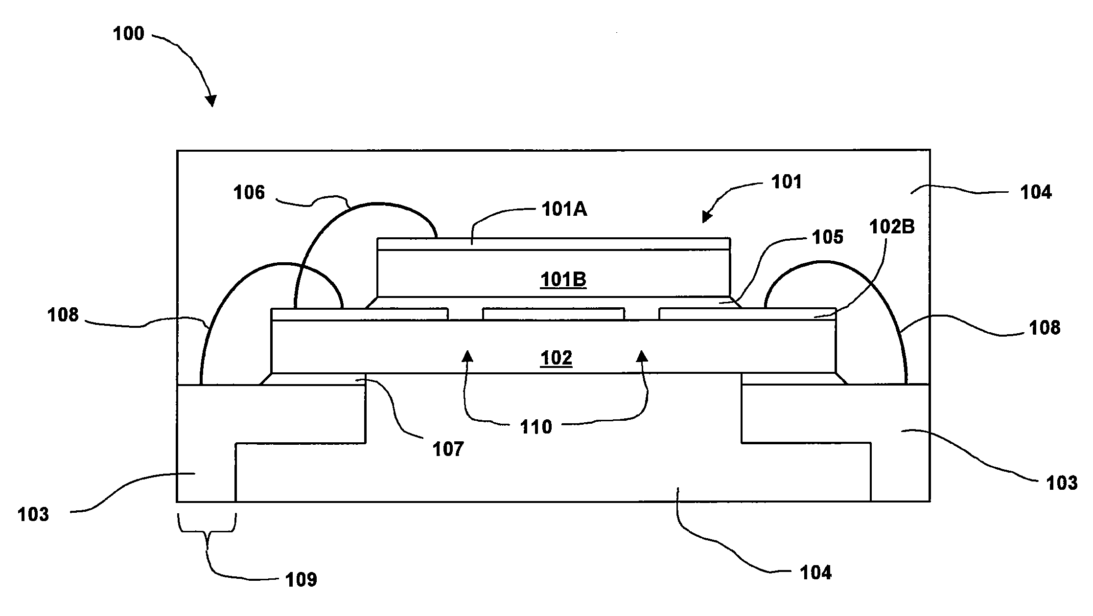
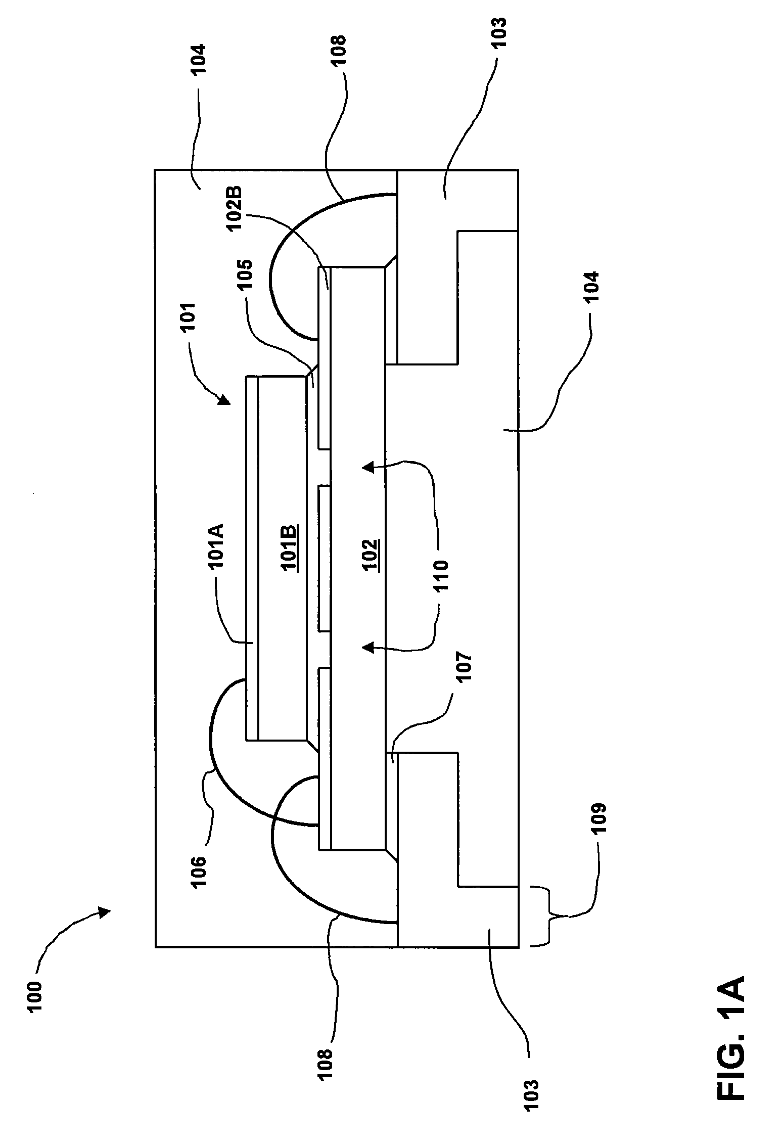
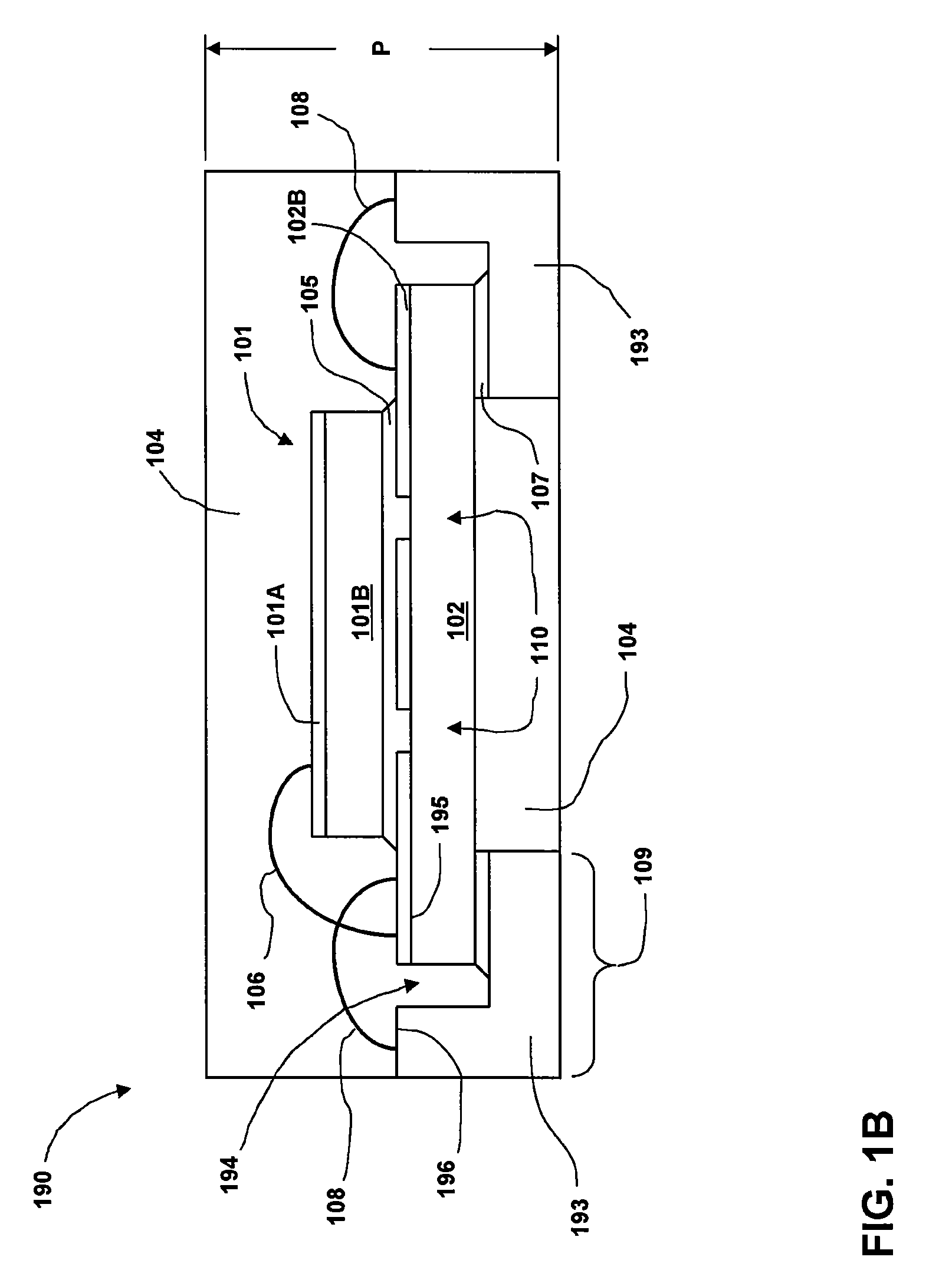
[0020]Embodiments of the invention contemplate stacked die package configurations for a MEMS resonator and its associated control chip that provide small package footprint and / or low package thickness. These stacked die package configurations further provide low thermal resistance and a robust electrically conductive path between the resonator chip and the control chip. Stacked die configurations include chip-on-lead (COL), chip-on-paddle (COP), and chip-on-tape (COT) packages. MEMS resonators contained in COL, COP, or COT stacked die packages, according to embodiments of the invention, may be beneficially used in lieu of quartz, ceramic, solid-state and other types of packaged timing references, due to the cost, reliability, and size constraints of these packaged timing references. In addition, the stacked die packages provided herein enable “drop-in” replacement of quartz packaged timing references used in existing applications, i.e., the form-factor and lead configuration of a pa...


PUM


Abstract

A stacked die package for an electromechanical resonator system includes a chip that contains an electromechanical resonator bonded onto the control chip for the electromechanical resonator by a thermally and / or electrically conductive epoxy. In various embodiments, the electromechanical resonator can be a micro-electromechanical system (MEMS) resonator or a nano-electromechanical system (NEMS) resonator. Packaging configurations that may include the chip that contains the electromechanical resonator and the control chip include chip-on-lead (COL), chip-on-paddle (COP), and chip-on-tape (COT) packages. The stacked die package provides small package footprint and / or low package thickness, as well as low thermal resistance and a robust conductive path between the chip that contains the electromechanical resonator and the control chip.

Description

CROSS-REFERENCE TO RELATED APPLICATIONS[0001]This application claims benefit of the United States provisional patent application titled, “Packages and / or Packaging Techniques for Microelectromechanical Devices,” filed on Jun. 15, 2006 and having Ser. No. 60 / 813,874. The subject matter of this related application is hereby incorporated herein by reference.BACKGROUND OF THE INVENTION[0002]1. Field of the Invention[0003]Embodiments of the present invention relate generally to the fabrication of packaged timing references and particularly to a packaging configuration for micro-electromechanical systems (MEMS) and nano-electromechanical systems (NEMS) resonator systems.[0004]2. Description of the Related Art[0005]Quartz resonator systems are used for timing applications in many electronic devices, including cell phones, automotive systems, game consoles, broadband communications, and almost any other digital product available. As quartz resonators decrease in size to meet the size constr...

Claims


Application Information

Patent Timeline
Patent Type & Authority Patents(United States)
IPC IPC(8): H01L23/48H01L23/34
CPCB81C1/00301H01L23/34H01L23/498B81C1/0023B81B7/007B81B2201/0271B81C2203/0154H01L23/3107H01L2224/48245H01L2224/48247H01L2924/01019H01L2924/10253H01L2924/1461H01L2224/73265H01L2224/48091H01L2924/00H01L2924/00014H01L2924/181H01L2924/00012H10N30/302B81B7/0077B81B7/0083B81B2207/094B81C1/00333B81C2203/0118B81B2207/07B81C1/00341B81C2201/016
Inventor GUPTA, PAVANRAZDA, ERIC
Owner SITIME
Why Eureka
Try Eureka