Minute structure and its manufacturing method

Active Publication Date: 2011-09-27
NIKON CORP
View PDF14 Cites 36 Cited by
  • Summary
  • Abstract
  • Description
  • Claims
  • Application Information

AI Technical Summary

Benefits of technology

[0007]Also, a structure that two or more DOE layers are stacked as in Patent Document 1 is assoc

Problems solved by technology

Where plural MLAs or DOEs are combined together, influence that is undesirable for an optical instrument such as a color shift or diffused reflection occurs if the accuracy of the alignment between optical elements is low.
In particular, in optical elements in a coupler for coupling optical fibers of 10 μm or less in diameter s

Method used


Image

  • Minute structure and its manufacturing method
  • Minute structure and its manufacturing method
  • Minute structure and its manufacturing method

Examples


first embodiment

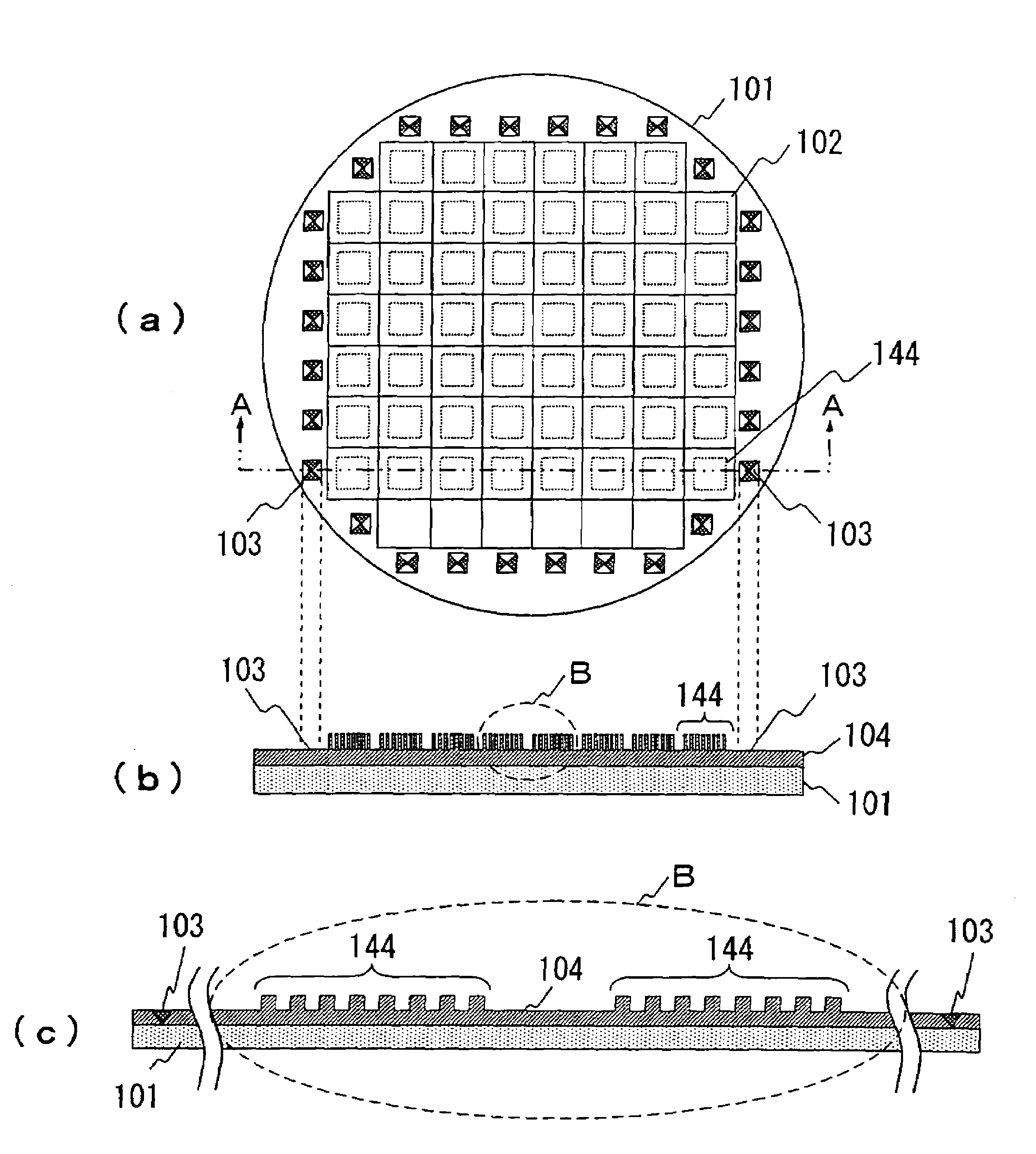
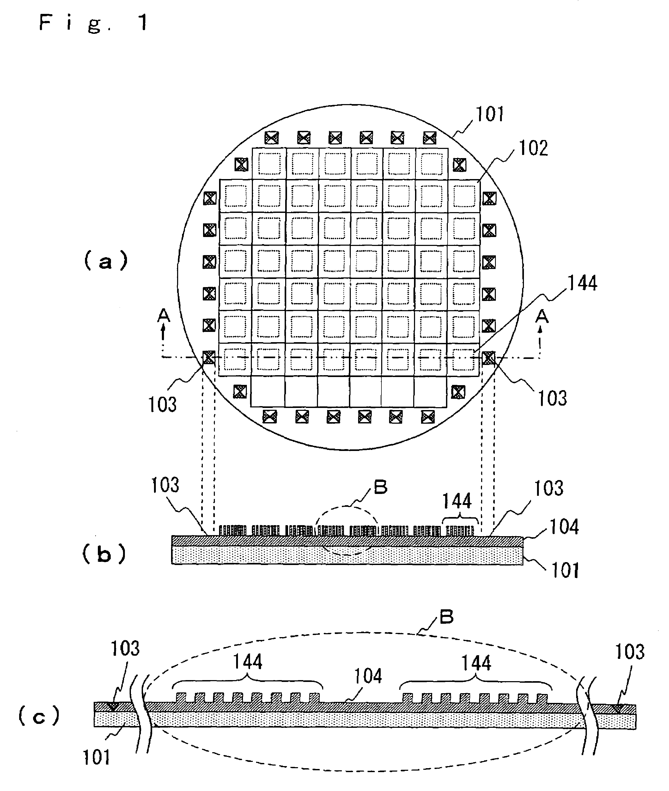
[0038]A first embodiment which relates to a minute structure and its manufacturing method according to the present invention will be described below with reference to FIGS. 1-3. FIG. 1 shows how plural minute structures are formed on a silicon wafer. Each minute structure which is manufactured according to the embodiment is used as an optical element and, in particular, is suitably used as a minute optical element formed on a semiconductor device.

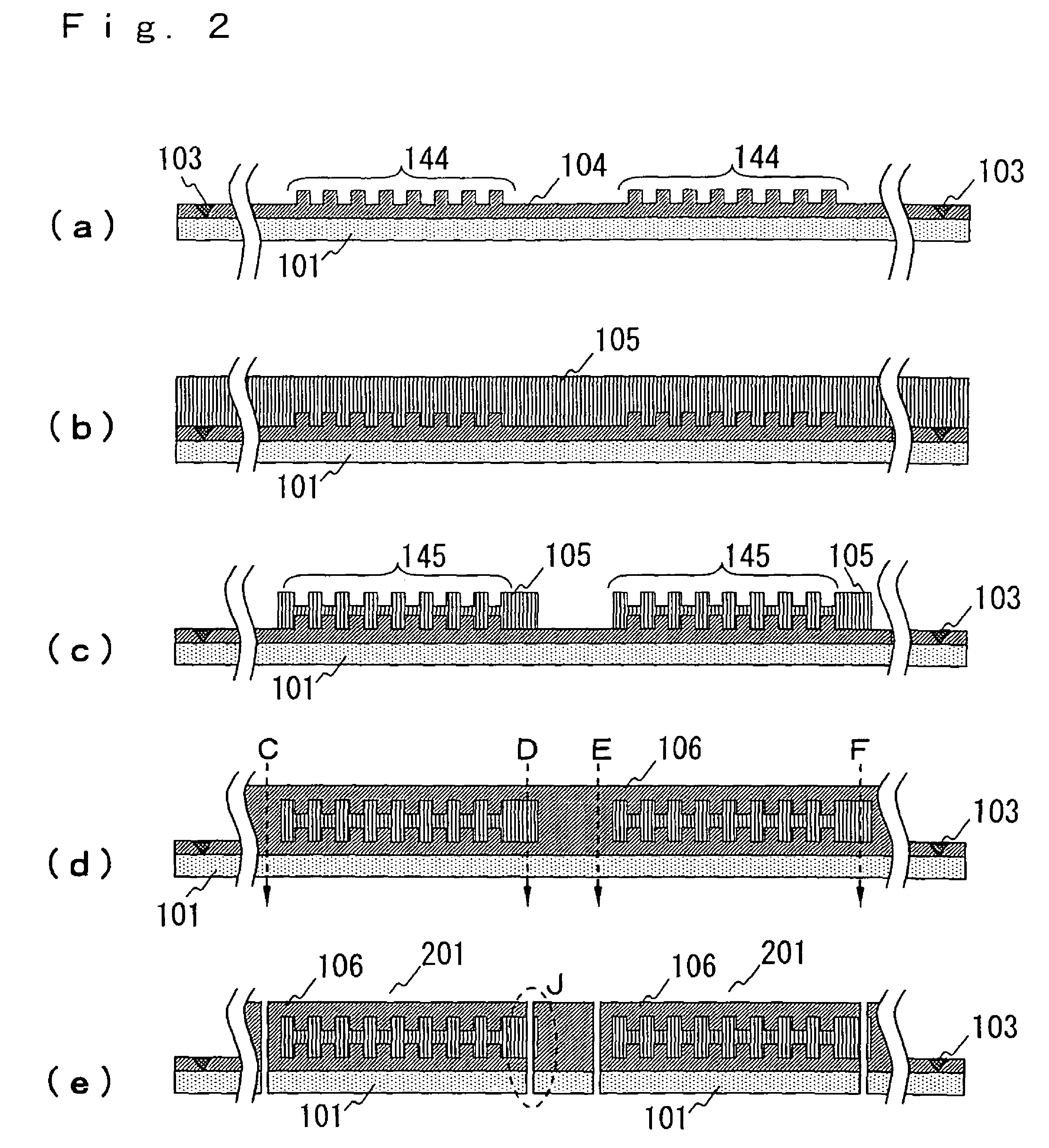
[0039]In FIG. 1, reference numeral 101 denotes a silicon wafer; 102, blocks in each of which one minute structure is formed; 103, alignment marks; 104, a first layer formed on the silicon wafer 101; and 144, pattern forming portions.

[0040]FIG. 1(a) is a top view of a silicon wafer 101. FIG. 1(b) is a sectional view taken at a cutting position A in FIG. 1(a). FIG. 1(c) is an enlarged view mainly showing a part indicated by a broken-line circle B in FIG. 1(b). A first layer 104 is formed on the silicon wafer 101 with a resin or the like, and ...

second embodiment

[0054]Next, a second embodiment relating to a minute structure and its manufacturing method will be described. A minute structure according to the second embodiment of the invention is configured in such a manner that a first member having concave alignment marks and a second member having convex alignment marks that are paired with the respective concave ones are fitted with and into each other. The minute structure manufactured by this embodiment is used as an optical element and, in particular, suitably used as a minute optical element formed on a semiconductor element.

[0055]The manufacturing method of the second embodiment will be outlined below. First, a mold master for one of the first member or the second member is produced by precision machining and a first reverse mold master is produced from the mold master by nanoimprinting or the like. Then, a sacrificial layer corresponding to a hollow portion is laid on the first reverse mold master, and patterned into a desired shape ...


PUM


Abstract

A manufacturing method of a minute structure having fine structures on opposing inner surfaces, includes the steps of forming a first pattern in a surface of a first layer, forming a sacrificial layer on the patterned surface of the first layer, forming a second pattern on a surface of the sacrificial layer, forming a second layer on the sacrificial layer and a portion of the surface of the first layer, and removing a member constituting the sacrificial layer. In the step of forming the first pattern on the first layer and the step of forming the second pattern on the sacrificial layer, the patterns are formed using the same alignment marks as references. This manufacturing method can realize highly accurate alignment even when plural lenses or DOEs are used.

Description

CROSS-REFERENCE TO RELATED APPLICATION[0001]This application is a U.S. National Stage application claiming the benefit of prior filed International Application Number PCT / JP2006 / 319718, filed Oct. 2, 2006, in which the International Application claims a priority date of Oct. 7, 2005 based on prior filed Japanese Application Number 2005-295490, the entire contents of which are incorporated herein by reference.TECHNICAL FIELD[0002]The present invention relates to a minute structure which is manufactured by using a semiconductor process as well as to its manufacturing method.BACKGROUND ART[0003]In recent years, semiconductor devices in which a resin structure is provided on a semiconductor element by using a semiconductor process have increased. For example, an MLA (microlens array) and a DOE (diffraction optical element) are known in which a lens is formed on an image sensor such as a CCD or a CMOS in an integral manner.[0004]In particular, plural MLAs or DOEs are used frequently for ...

Claims


Application Information

Patent Timeline
IPC IPC(8): G02B5/18B81C99/00
CPCB81C99/0085G02B3/0025G02B3/0075G02B5/1819G02B5/1852G02B27/4277B81B2201/047G02B3/0068Y10S359/90
Inventor HAYASHI, MASATOSHI
Owner NIKON CORP
Why Eureka
Try Eureka