Device for polishing peripheral edge of semiconductor wafer

a technology for peripheral edges and semiconductor wafers, which is applied in the direction of grinding drives, grinding machine components, manufacturing tools, etc., can solve the problems of large equipment space, adversely affecting the yield of device wafers, and large equipment space, so as to reduce the space required for the apparatus, maintain constant tension in the tape, and shorten the polishing time

Active Publication Date: 2011-10-04
EBARA CORP +1
View PDF13 Cites 11 Cited by
  • Summary
  • Abstract
  • Description
  • Claims
  • Application Information

AI Technical Summary

Benefits of technology

[0008]It is therefore an object of this invention, which relates to the processing of the peripheral part a semiconductor wafer, to provide a device for polishing the notch and the beveled part of a semiconductor wafer efficiently within a single device.
[0009]It is another object of this invention to provide such a device with which the polishing time can be shortened and the space required for the apparatus can be reduced.
[0010]It is a third object of this invention to provide such a device capable of positioning a semiconductor wafer accurately on a wafer stage.

Problems solved by technology

Such conventional methods have problems because the notch and the beveled part of a semiconductor wafer are polished independently such that it takes too long to transport the wafer between these two devices and this requires a large space for the equipment.
There is also the problem of the semiconductor wafer becoming dry while being transported, adversely affecting the yield of device wafers.
The positioning of a semiconductor wafer on the wafer stage in each polishing device is carried out by means of a pair of chuck handles of a robot for transporting wafers but since a plurality of cylinders are used for improved accuracy in the positioning, a large space is required for the equipment.
Since air cylinders are used for the purpose, furthermore, an error on the order of 0.5 mm arises in the positioning.
There is still another problem that an excessive grasping force is applied on the peripheral edge of the wafer and tends to damage the edge portion of the wafer.
This gives rise to the problem of deforming or damaging the semiconductor wafer.
Since the outer diameter of the tape is determined by the presence or absence of light from a light emitter received by a plurality (usually eight) of sensors of a light receiving part arranged at the side of the tape supply roll, the torque value of the motor changes in a stepwise manner, giving rise to the problem of the tension in the tape not being constant.

Method used


Image

  • Device for polishing peripheral edge of semiconductor wafer
  • Device for polishing peripheral edge of semiconductor wafer
  • Device for polishing peripheral edge of semiconductor wafer

Examples


Embodiment Construction

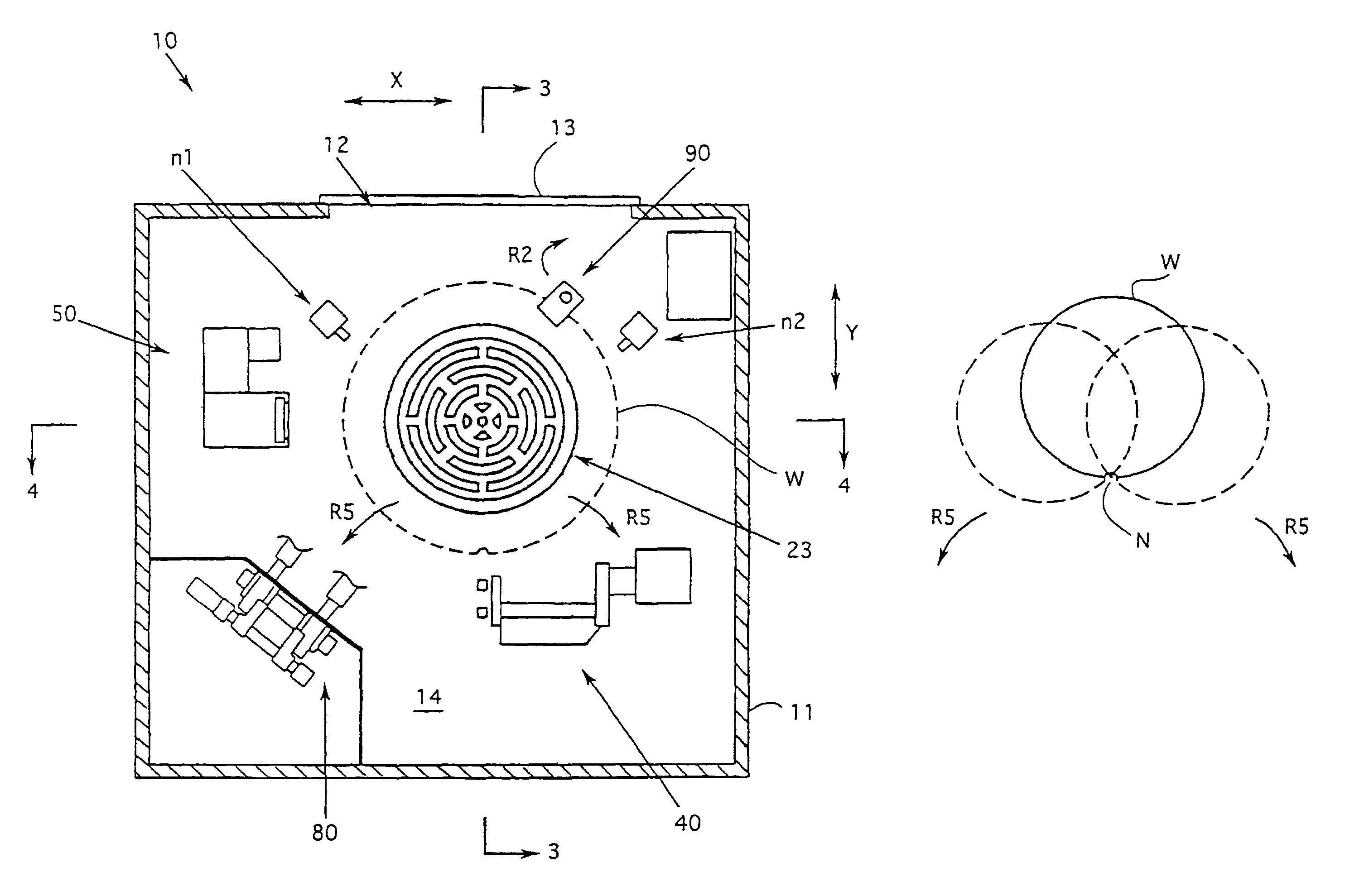
[0061]A device according to this invention is for polishing the peripheral edge part of a semiconductor wafer (inclusive of the notch and the beveled part).

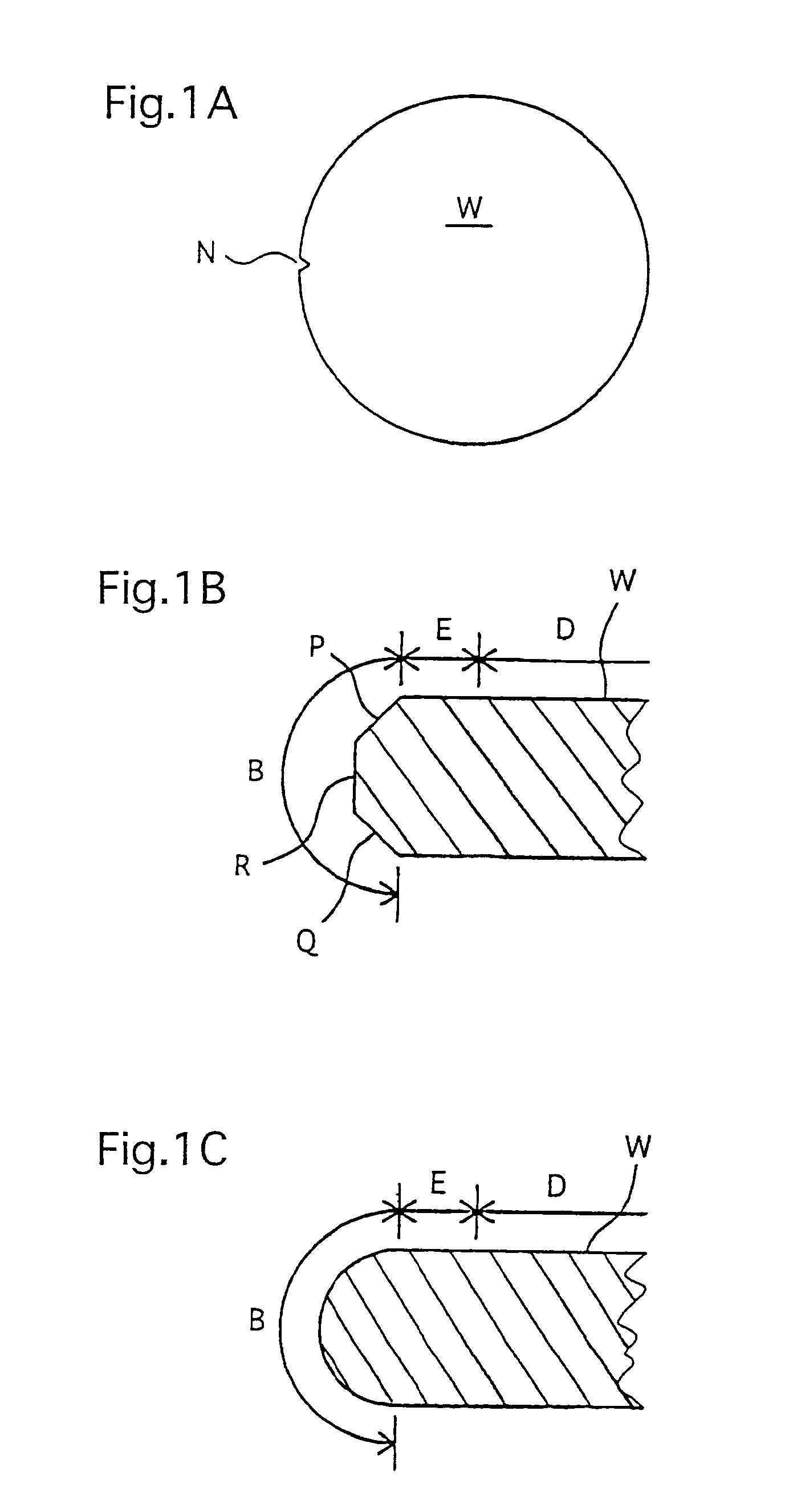
[0062]As shown in FIG. 1A, the semiconductor wafer (hereinafter referred to simply as the wafer) W is a thin disk comprising monocrystalline silicon and a notch N is provided to its periphery for indicating its orientation, serving as an a reference for positioning the circularly shaped wafer W inside a semiconductor processing apparatus.

[0063]The wafer W may be roughly classified either as a straight type or a round type, depending on its cross-sectional shape. A semiconductor wafer of a straight type has a polygonal sectional shape as shown in FIG. 1B, while a semiconductor wafer of a round type has a curved (semicircular or semi-elliptical) sectional shape as shown in FIG. 1C.

[0064]Throughout herein, expression “beveled part” will be used, in the case of a wafer W of a straight type shown in FIG. 1B, to indicate the upper slop...


PUM

PropertyMeasurementUnit
diameteraaaaaaaaaa
rotational speedaaaaaaaaaa
rotary speedaaaaaaaaaa

Abstract

A device for polishing the peripheral edge part of a semiconductor wafer includes a wafer stage for holding the wafer, a wafer stage unit including devices for rotating the wafer stage, causing the wafer stage to undergo a rotary reciprocating motion within the same plane as the surface of the wafer stage, and moving the wafer stage parallel to the surface, a notch polishing part for polishing the notch on the wafer and a bevel polishing part for polishing the beveled part of the wafer. Pure water is supplied to the wafer to prevent it from becoming dry as it is transported from the notch polishing part to the bevel polishing part.

Description

[0001]This application is a continuation of International Application No. PCT / JP2006 / 308492 filed Apr. 18, 2006, that was amended on Sep. 14, 2006 and claims priority on Japanese Patent Application 2005-121464 filed Apr. 19, 2005.TECHNICAL FIELD[0002]This invention relates to a device for polishing the peripheral edge part (including the notch and the beveled part) of a semiconductor wafer.BACKGROUND ART[0003]The peripheral edge part of a semiconductor wafer is conventionally polished by independently using a device for polishing the notch part (as disclosed in Japanese Patent Publication Tokkai 9-85599) and another device for polishing the beveled part (as disclosed in Japanese Patent Publications Tokkai 7-164301 and 8-174399). The polishing of the peripheral part is carried out by a so-called wet method whereby a polishing liquid in a slurry form obtained by dispersing abrading particles in water or a water-based reactive liquid is supplied to the target part to be polished (such ...

Claims


Application Information

Patent Timeline
Patent Type & Authority Patents(United States)
IPC IPC(8): B24B49/00B24B9/00B24B21/00B24B49/12B24B55/08H01L21/304
CPCB24B21/16B24B9/065H01L21/304
Inventor TAKAHASHI, TAMAMIITO, KENYASHIRAKASHI, MITSUHIKOINOUE, KAZUYUKIYAMAGUCHI, KENJISEKI, MASAYASATO, SATORUWATANABE, JUNKATO, KENJITAMURA, JUNASAKAWA, SOUICHI
Owner EBARA CORP
Why Eureka
Try Eureka