Method for reducing crystal defect of SIMOX wafer and SIMOX wafer

a technology of simox wafer and crystal defect, which is applied in the direction of basic electric elements, electrical apparatus, semiconductor devices, etc., can solve the problems of wafers prone to crystal defects, thermal stress, and crystal defects remaining in the silicon layer underneath the box layer that cannot be ignored, so as to reduce the density of crystal defects, confirm the effect of reducing crystal defects, and reduce crystal defects

Inactive Publication Date: 2011-10-04
SUMCO CORP
View PDF7 Cites 0 Cited by
  • Summary
  • Abstract
  • Description
  • Claims
  • Application Information

AI Technical Summary

Benefits of technology

[0009]Hence, it is an object of the present invention to reduce crystal defects present in a silicon layer underneath the BOX layer of a SIMOX wafer.
[0012]Here in the first step, it is necessary to provide, as implantation energy, such a degree of energy to ions as to cause the ions to reach to at least a preset depth of the SIMOX wafer. Consequently, ions that have reached the preset depth collide with crystal defects and the kinetic energy of the ions acts on the crystal defects in such a direction as to collapse the form thereof. Accordingly, by subsequently performing a high-temperature heat treatment to provide thermal energy to the crystal defects, it is possible to easily restore the crystallinity thereof. Note here that the temperature conditions and the dose of ion implantation relate to the amount of reduction in crystal defects. Therefore, the implantation temperature may be controlled and the dose may be set consistently with the density of targeted crystal defects.
[0013]More specifically, the method includes: a first step of colliding ions implanted into the silicon layer underneath the buried oxide film from a surface of the SIMOX wafer against crystal defects to destroy the crystal defects; and a second step of heating the SIMOX wafer following this first step to recrystallize the silicon layer. As described above, by destroying the crystal defects and then heating the SIMOX wafer up to a recrystallization temperature of the silicon layer, it is possible to more effectively restore the crystallinity of the crystal defects.
[0015]In addition, the second step is intended to heat the SIMOX wafer to a temperature of 1150° C. or higher but not higher than 1350° C. By heating the SIMOX wafer to such a high-temperature, the recrystallization of crystal defects is allowed to progress easily also in terms of thermodynamics. Thus, it is possible to restore crystallinity in a short period of time.
[0020]Here, in order to confirm the effect of reducing crystal defects in accordance with the second aspect, a sum of doses at the respective times of ion implantation in the second aspect was first made to agree with the dose at the time of ion implantation in the first aspect. Then, ion implantation was performed a plural number of times with different amounts of implantation energy. After that, an examination was made of an oxygen concentration distribution in the depth direction in a predetermined depth region of the silicon layer underneath the buried oxide film. Then, it was confirmed that the oxygen concentration distribution was made uniform. Next, this SIMOX wafer was heat-treated and an examination was made of the density of crystal defects in a predetermined depth region of the silicon layer underneath the buried oxide film. Then, it was confirmed that the density of crystal defects decreased, compared with the density in the first aspect. Accordingly, it has proved that, by implanting ions separately a plural number of times with different amounts of implantation energy into a predetermined depth region of the silicon layer underneath the buried oxide film and thereby making the oxygen concentration distribution uniform in the depth direction, it is possible to reduce crystal defects with higher efficiency. In addition, it has been confirmed that, since the oxygen concentration distribution can be made uniform by performing ion implantation a plural number of times with different amounts of implantation energy as described above, the second aspect has the advantage of being able to decrease the total dose of ions to be implanted to reduce crystal defects.
[0021]In this case, if the ions implanted into the silicon layer underneath the buried oxide film are, for example, oxygen ions, then the first step initiates ion implantation with the temperature of the SIMOX wafer being 50° C. or lower, and sets conditions at the respective times of ion implantation, so that the ion dose is 1×10¹⁵ atoms / cm2 to 1.5×10¹⁶ atoms / cm2 and the implantation energy is 150 keV to 220 keV. Here, the ion dose is determined according to the density of crystal defects remaining in the silicon layer, the frequency of ion implantation, and the like. The implantation energy is determined according to the type of ion element, an implantation depth, and the like. By carrying out the first step under such conditions as described above, it is possible to efficiently destroy crystal defects present in the silicon layer underneath the buried oxide film. In addition, in the first step, the temperature of a pre-ion implantation SIMOX wafer is preferably low and is desirably set to, for example, 50° C. or lower, in order to retain the form of crystal defects broken by colliding ions against the defects.

Problems solved by technology

However, the crystal defects remaining in the silicon layer underneath the BOX layer have become an issue that can no longer be ignored due to the miniaturization of devices.
Consequently, a temperature difference arises in the thickness direction of the wafer, thus causing thermal stress.
This makes the wafer prone to a crystal defect, particularly a slip dislocation.
Here, if many crystal defects remain in the silicon layer underneath the BOX layer of an SOI wafer, at the time of LSA-based heat treatment, many slip dislocations occur in the silicon layer.
As a result, there may arise the warpage deformation of the wafer due to internal strain.
Such the warpage deformation of the wafer adversely affects a device process and may cause a yield to degrade.

Method used


Image

  • Method for reducing crystal defect of SIMOX wafer and SIMOX wafer
  • Method for reducing crystal defect of SIMOX wafer and SIMOX wafer
  • Method for reducing crystal defect of SIMOX wafer and SIMOX wafer

Examples


first embodiment

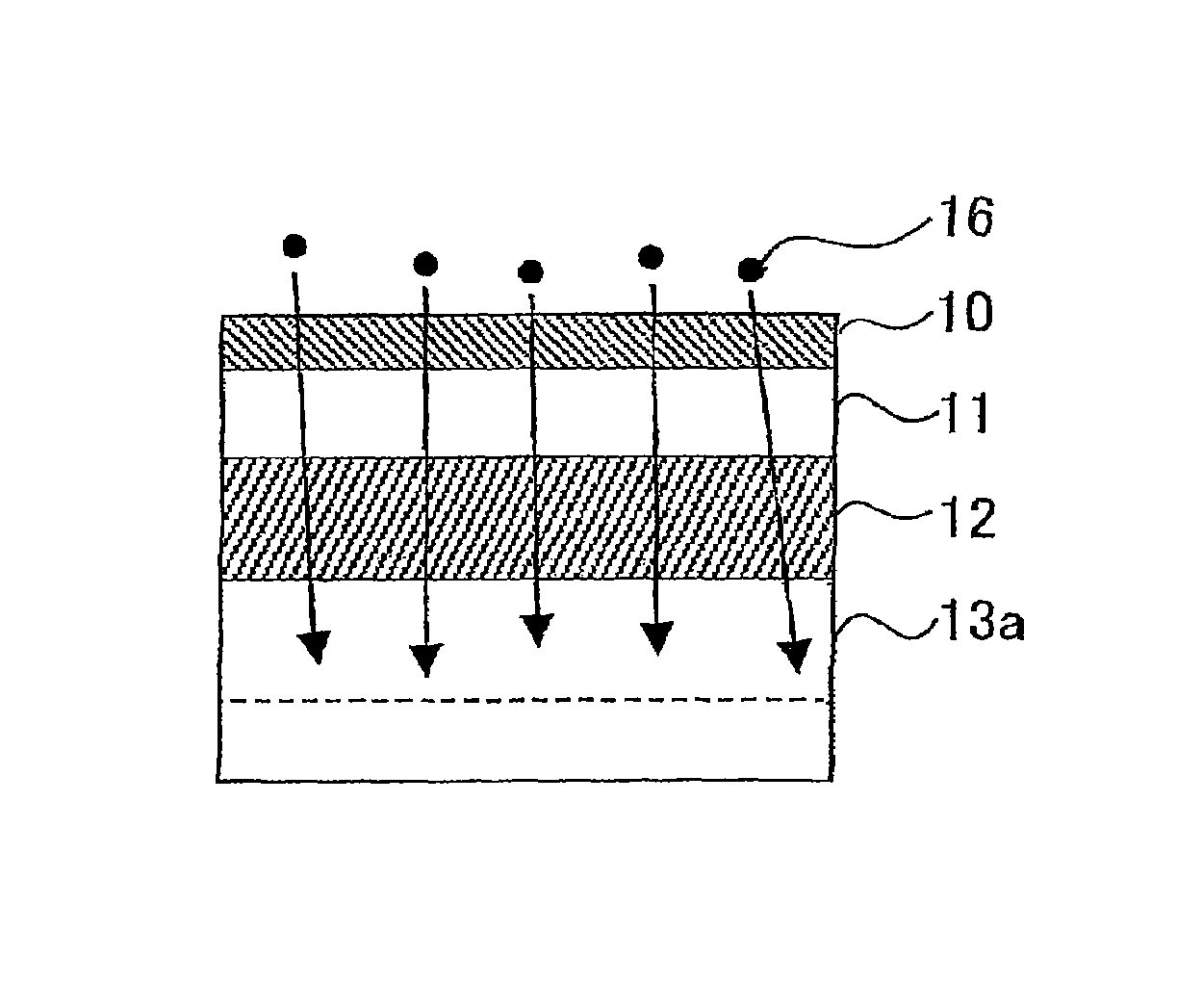
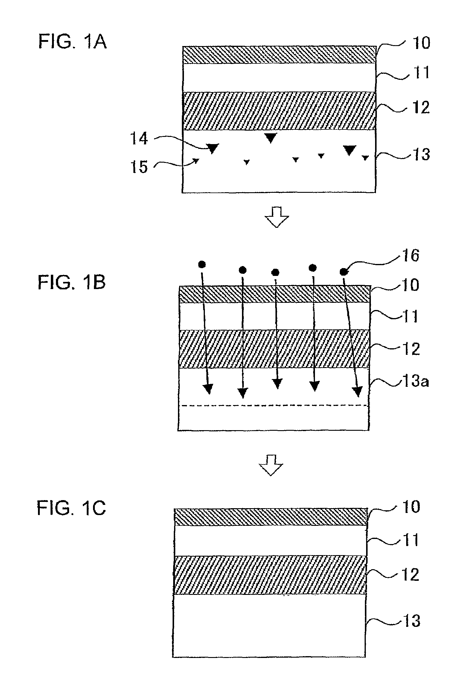
[0028]FIG. 1 is a schematic view used to explain a method for reducing the crystal defects in a SIMOX wafer to which a first embodiment of the present invention is applied. The method for reducing the crystal defects in accordance with the present invention is intended for a SIMOX wafer manufactured using a SIMOX method. The method for manufacturing the SIMOX wafer is constituted by including a step of implanting oxygen ions into a silicon wafer and a step of performing a predetermined heat treatment on this silicon wafer. Any SIMOX wafers can be covered by the present invention as long as the wafers are manufactured by including these steps, even if the conditions of the respective steps differ. Consequently, SIMOX wafers manufactured using an MLD (Modified Low Dose) method, an ITOX (Internal Thermal OXidation) method, and the like can also be covered by the present invention.

[0029]In the present embodiment, an explanation will be made by taking, as an example, a SIMOX wafer manufa...

example 1

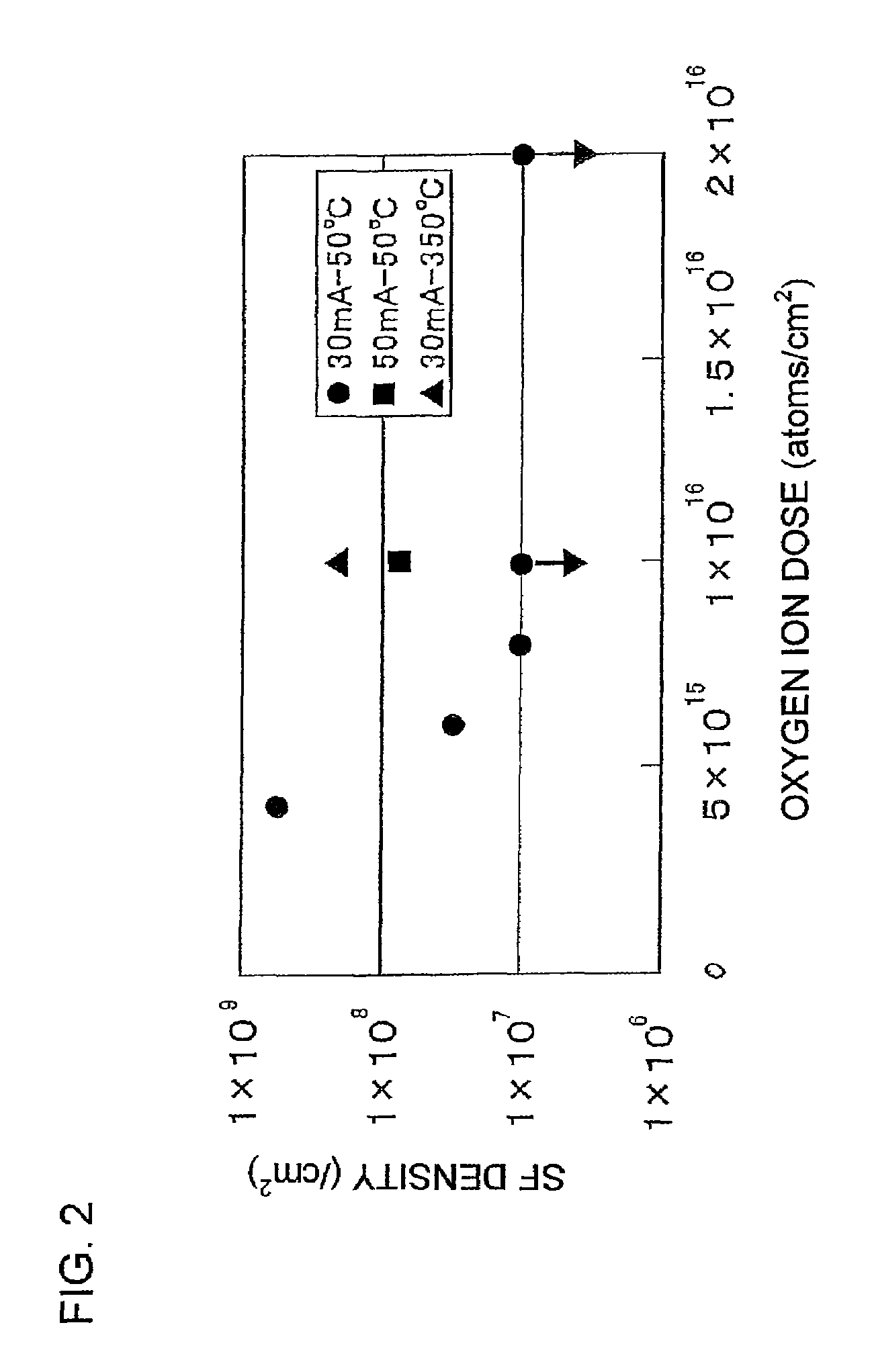
[0048]FIG. 2 is a graphical view used to explain a relationship between the dose of oxygen ions implanted into a SIMOX wafer and an SF density. The horizontal axis of the figure represents an oxygen ion dose (atoms / cm2) and the vertical axis represents the SF density ( / cm2) of a depth region of a silicon layer. Here, the depth region refers to a region 200 nm deep from a boundary between a BOX layer and the silicon layer.

[0049]In the present example, a prepared SIMOX wafer was first cleaned and dried, and then housed in an ion implantation apparatus to maintain the temperature of the SIMOX wafer at 50° C. Then, implantation energy was fixed to 216 keV and, under five test conditions in which ion doses were 4×10¹⁵ atoms / cm2, 6×10¹⁵ atoms / cm2, 8×10¹⁵ atoms / cm2, 1×10¹⁶ atoms / cm2 and 2×10¹⁶ atoms / cm2, oxygen ions were implanted for the respective test conditions. Here, a current value detected by a current detection section of the ion implantation apparatus at the time of ion implantati...

example 2

[0052]Next, oxygen ions were implanted (at a current value of 30 mA) into a pre-ion implantation SIMOX wafer with the temperature thereof raised to 350° C., by setting the implantation energy to 216 keV and the oxygen ion dose to 1×10¹⁶ atoms / cm2. Thus, there was evaluated the SF density of the SIMOX wafer treated under the same heat treatment conditions as those in Example 1. The result of this evaluation is represented by the symbol Δ and is shown in FIG. 2. From the result of FIG. 2, it was confirmed that if the temperature of a pre-ion implantation wafer was made higher, the decrement of the SF density reduced. The reason for this is that, as the result of ion implantation being performed at a high temperature, SFs do not fully vanish since recrystallization progresses during implantation. Accordingly, it is preferable to maintain the temperature of a pre-ion implantation SIMOX wafer at 50° C. or lower.


PUM


Abstract

The method includes: a first step of colliding ions implanted from a surface of a SIMOX wafer into a silicon layer underneath a BOX layer against crystal defects to destroy the crystal defects; and a second step of heating the wafer obtained in the first step to recrystallize the silicon layer. If the ions to be implanted into the silicon layer are oxygen ions, then the first step initiates ion implantation with the temperature of the SIMOX wafer being 50° C. or lower, and sets an ion dose to 5×10¹⁵ atoms / cm2 to 1.5×10¹⁶ atoms / cm2 and implantation energy to 150 keV or higher but not higher than 220 keV. Consequently, crystal defects present in the silicon layer underneath the BOX layer of the SIMOX wafer are reduced.

Description

BACKGROUND OF THE INVENTION[0001]1. Field of the Invention[0002]The present invention relates to a method for reducing the crystal defects in a SIMOX (Separation by IMplanted OXygen) wafer and to the SIMOX wafer and, more particularly, to a technique for reducing crystal defects present in a silicon layer underneath a buried oxide film of the SIMOX wafer.[0003]2. Description of the Related Art[0004]Conventionally, as one of methods for manufacturing an SOI (Silicon On Insulator) wafer, a SIMOX method has been known, in which oxygen ions are implanted from at least one of the surfaces of a silicon wafer, and then a high-temperature heat treatment is performed, thereby forming a buried oxide film (hereinafter referred to as a BOX (Buried Oxide) layer) by the implanted oxygen ions. The SIMOX wafer thus manufactured is generally shipped to a device manufacturer with a surface oxide film removed. A surface SOI layer and a BOX layer thereunder are utilized in a device manufacturing proces...

Claims


Application Information

Patent Timeline
Patent Type & Authority Patents(United States)
IPC IPC(8): H01L21/32
CPCH01L21/3226H01L21/76243H01L29/32
Inventor KASAMATSU, RYUSUKE
Owner SUMCO CORP
Why Eureka
Try Eureka