LED (light-emitting diode) and manufacturing method thereof

A technology of light-emitting diodes and manufacturing methods, which is applied in semiconductor/solid-state device manufacturing, semiconductor devices, electrical components, etc., can solve the problems of low light-emitting efficiency of light-emitting diodes, and achieve the goal of improving external quantum efficiency, increasing reflection, and improving light utilization. Effect

Inactive Publication Date: 2011-04-20
XIAN SHENGUANG ANRUI PHOTOELECTRIC TECH
View PDF4 Cites 6 Cited by
  • Summary
  • Abstract
  • Description
  • Claims
  • Application Information

AI Technical Summary

Problems solved by technology

[0007] The object of the present invention is to provide a light-emitting diode to solve the problem of low light extraction efficiency of the existing light-emitting diodes

Method used


Image

  • LED (light-emitting diode) and manufacturing method thereof
  • LED (light-emitting diode) and manufacturing method thereof
  • LED (light-emitting diode) and manufacturing method thereof

Examples


Embodiment Construction

[0030] In order to make the above objects, features and advantages of the present invention more comprehensible, specific implementations of the present invention will be described in detail below in conjunction with the accompanying drawings.
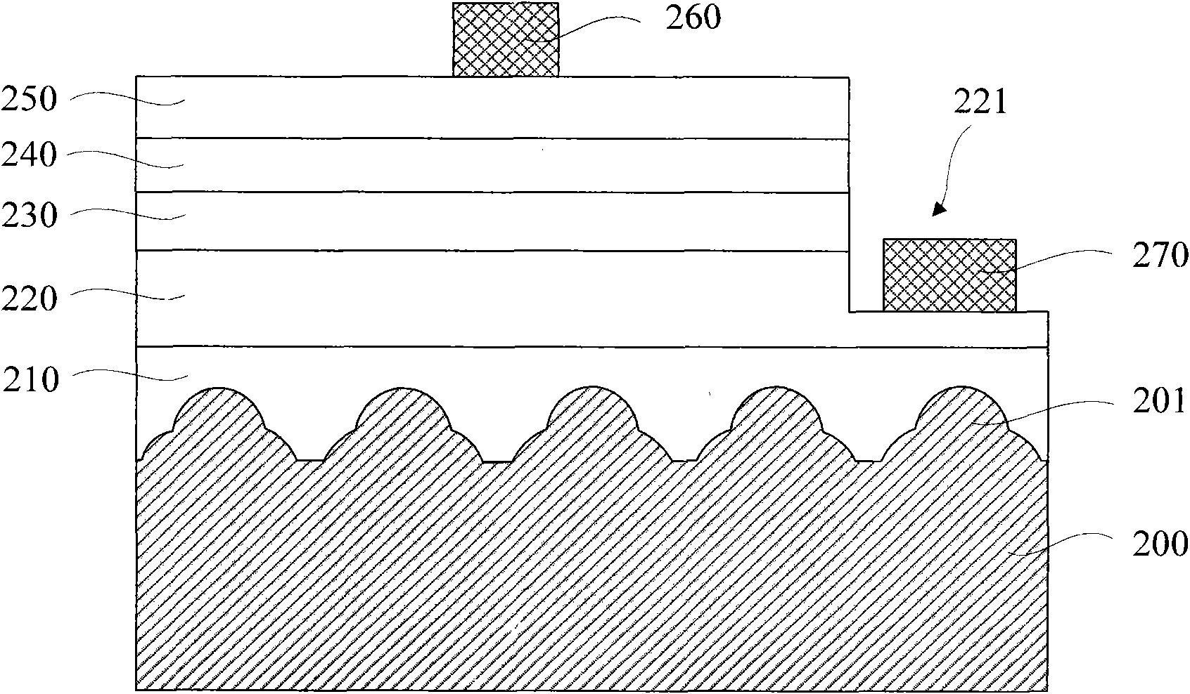
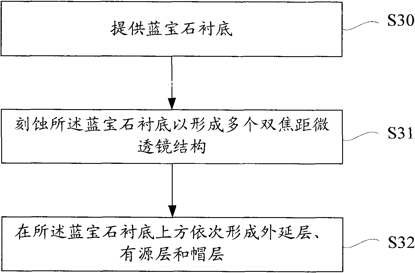
[0031] The core idea of ​​the present invention is to provide a light-emitting diode, which includes: a sapphire substrate; an epitaxial layer, an active layer and a cap layer sequentially located above the sapphire substrate; wherein the sapphire substrate is close to the epitaxial The surface of the layer has a plurality of bifocal microlens structures. The double-focal-length microlens structure can increase the reflection of light, improve the external quantum efficiency of the light-emitting diode, thereby improving the light utilization rate of the light-emitting diode; The lattice matching degree of the film layer reduces the crystal defects of the film layer formed on the sapphire substrate, improves the internal quantum effici...


PUM


Abstract

The invention discloses an LED (light-emitting diode) and a manufacturing method thereof, wherein the LED comprises a sapphire substrate, an epitaxial layer, an active layer and a cap layer, which are sequentially positioned above the sapphire substrate, wherein, a plurality of bifocal lenticule structures are arranged on the surface of the sapphire substrate, which is near to the epitaxial layer. The bifocal lenticule structures can increase the reflection of light of the sapphire substrate, improve external quantum efficiency of the LED, and further improve light utilization ratio of the LED; moreover, as a plurality of bifocal lenticule structures are formed, lattice matching degree between the sapphire substrate and other membranous layers can be improved, the crystal defect of the membranous layers formed on the sapphire substrate is reduced, and internal quantum efficiency of the LED is improved.

Description

technical field [0001] The invention relates to the field of semiconductor light emitting, in particular to a light emitting diode and a manufacturing method thereof. Background technique [0002] Light Emitting Diode (LED, Light Emitting Diode) is used in various fields due to its advantages of long life and low energy consumption, especially as its lighting performance index is greatly improved day by day, LED is often used as a light emitting device in the lighting field. Among them, gallium nitride (GaN) is the representative III-V compound semiconductor due to its wide band gap, high luminous efficiency, high electron saturation drift speed, and stable chemical properties. The field of optoelectronic devices has great application potential and has attracted widespread attention. [0003] However, the current semiconductor light-emitting diodes have the problem of low luminous efficiency. For ordinary unpackaged light-emitting diodes, the light extraction efficiency is...

Claims


Application Information

Patent Timeline
Patent Type & Authority Applications(China)
IPC IPC(8): H01L33/58H01L33/12H01L33/42H01L33/00
CPCH01L21/0242H01L21/0254H01L33/04H01L33/007H01L21/02658H01L33/02H01L21/02458H01L21/0243H01L33/20
Inventor 牛崇实张翼德
Owner XIAN SHENGUANG ANRUI PHOTOELECTRIC TECH
Why Eureka
Try Eureka