

Wired circuit board with interposed metal thin film and producing method thereof
a technology of wired circuit boards and metal thin films, which is applied in the direction of double resist layers, instruments, record information storage, etc., can solve the problems of corrosion and discoloration of copper conductive layers, and achieve the effects of preventing corrosion and discoloration of terminal portions, forming easily and reliably, and preventing migration of conductive patterns
- Summary
- Abstract
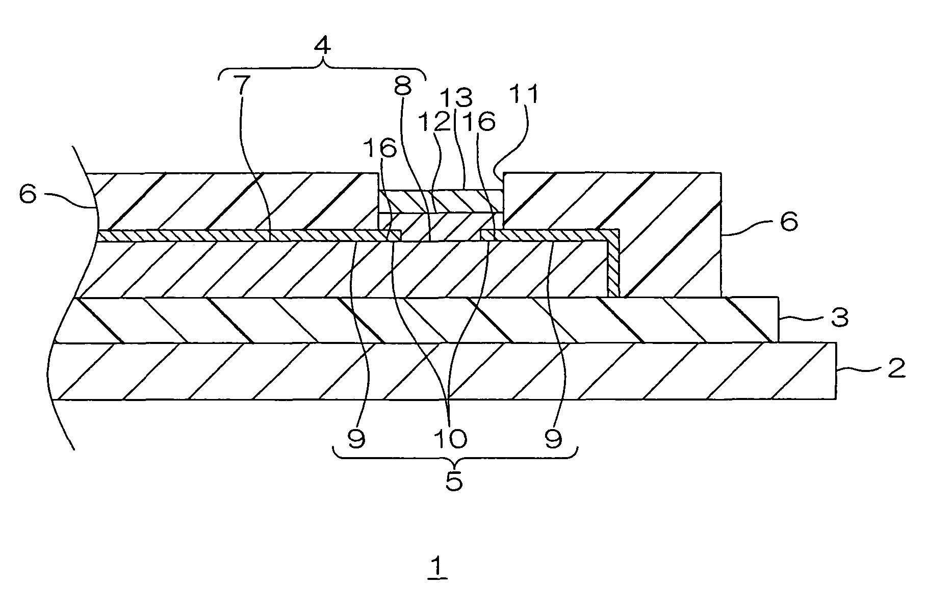
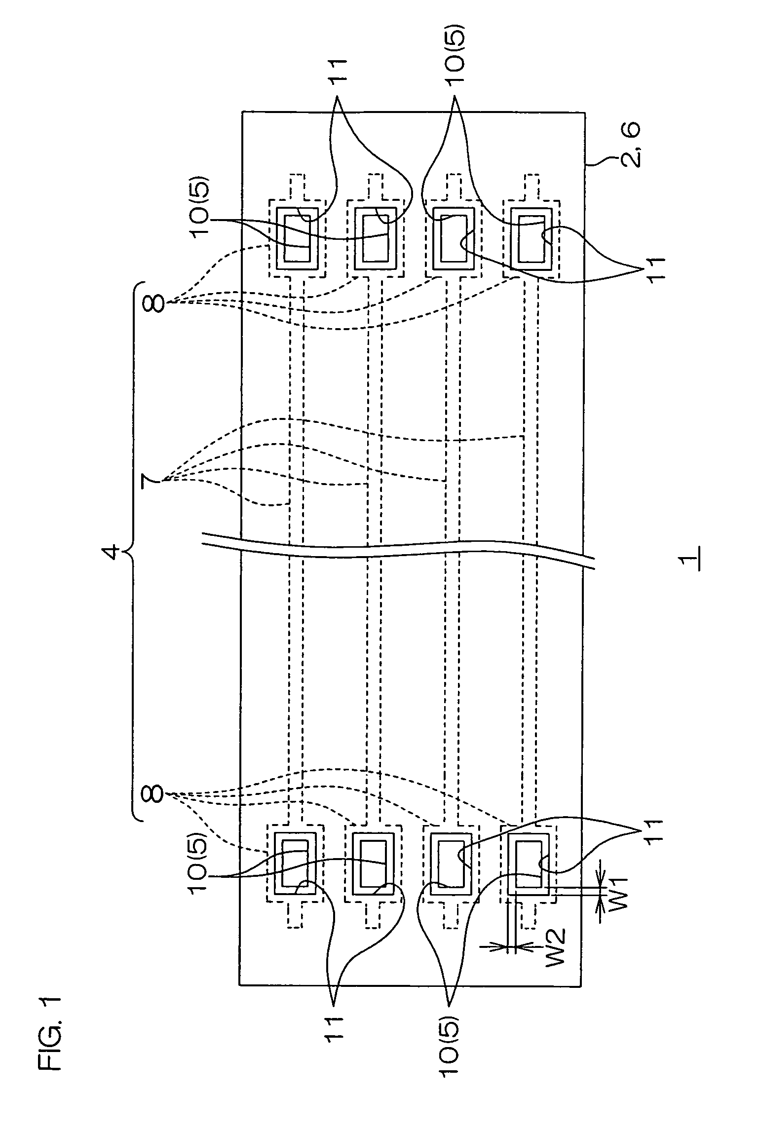
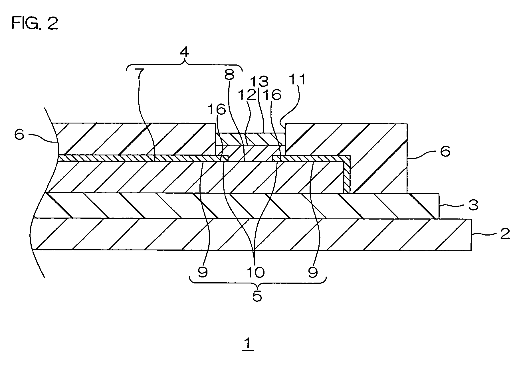
- Description
- Claims
- Application Information
AI Technical Summary
Benefits of technology
Problems solved by technology
Method used
Image

Examples
example 1
[0095]A metal supporting board made of a stainless steel foil having a thickness of 20 μm was prepared (see FIG. 3(a)).
[0096]Then, a varnish of a photosensitive polyamic acid resin was uniformly coated on the surface of the metal supporting board using a spin coater. Then, the coated varnish was heated at 90° C. for 15 minutes to form a base coating. Thereafter, the base coating was exposed to light at 700 mJ / cm2 via a photomask, heated at 190° C. for 10 minutes, and then developed using an alkaline developer. Subsequently, the base coating was cured at 385° C. under a reduced pressure of 1.33 Pa to form an insulating base layer made of polyimide in a pattern corresponding to a portion where a conductive pattern was formed on the metal supporting board (see FIG. 3(b)). The thickness of the insulating base layer was 10 μm.
[0097]Then, the conductive pattern made of copper and having a thickness of 10 μm was formed by an additive method in a wired circuit pattern integrally including w...
PUM
| Property | Measurement | Unit |
|---|---|---|
| width | aaaaa | aaaaa |
| width | aaaaa | aaaaa |
| width | aaaaa | aaaaa |
Abstract
Description
Claims
Application Information