Plasmon shield to shape and reduce optical spot

a plasmon shield and optical spot technology, applied in the field of magnetic read/write heads, can solve the problems of difficult to obtain a spot size less than 50 nm, difficult to fabricate a sharp tip with a 5 nm tip radius, and difficult to achieve alignment, etc., to achieve the effect of reducing the optical spot siz

Active Publication Date: 2011-10-11
HEADWAY TECH INC
View PDF10 Cites 34 Cited by
  • Summary
  • Abstract
  • Description
  • Claims
  • Application Information

AI Technical Summary

Benefits of technology

[0015]One objective of the present invention is to minimize the optical spot size produced in a magnetic medium by an edge plasmon generator (EPG) without scaling down the tip size and changing the tip angle of the EPG.
[0016]A second objective of the present invention is to minimize the optical spot size in an EPG design without significantly affecting the plasmon mode and without reducing the overall optical efficiency.
[0017]These objectives are achieved in various embodiments of the present invention wherein a TAMR write head comprises a main pole that has an edge plasmon generator (EPG) adjoining a trailing portion of a pole tip region along the ABS and extending a certain distance along a surface of the main pole towards the back end of the write head. Preferably, the EPG has a triangular design having two sides made of a plasmon layer comprising a highly conductive, non-magnetic metal that intersect at a vertex which is substantially a straight edge. The third side of the triangular shape and a core formed between the two EPG sides is made of a magnetic material. The third side and core may be considered the leading portion of the main pole layer and are generally made of the same magnetic material as in the main pole. In all embodiments, the vertex is essentially formed perpendicular to the ABS and faces a waveguide that is formed with an end at the ABS or recessed a certain distance from the ABS to reduce optical leakage. The waveguide extends in a lengthwise direction parallel to a lengthwise direction of the EPG that is towards the back end of the TAMR head. EPG sides are covered with a dielectric layer separating the EPG and waveguide and having a low index of refraction in order to enable efficient optical radiation transfer from the waveguide to EPG. A key feature of the present invention is a plasmon shield formed between an end of the waveguide facing the ABS and the EPG thereby enabling a smaller optical spot size to be focused on the magnetic medium during a writing process. The plasmon shield is made of a noble metal with a thin skin depth to shunt the electric field and maintain the edge plasmon mode in the vicinity of the EPG vertex to provide improved optical efficiency. The plasmon shield has a first surface along the ABS and a second surface facing the vertex and separated from the vertex and EPG sides by the aforementioned dielectric layer.
[0018]From a cross-sectional view that shows TAMR head components having a height dimension in a direction perpendicular to the ABS, the second surface of the plasmon shield and a surface of the waveguide facing the EPG form a plane that is perpendicular to the ABS. The waveguide generally extends to the back end of the TAMR head and has a height significantly larger than that of the EPG. In one embodiment, the interface between the waveguide and plasmon shield may be formed parallel to the ABS. In a preferred embodiment for improved optical efficiency, the surface of the plasmon shield opposite the ABS and including the interface with the waveguide is sloped with respect to the ABS such that the height of the second surface is less than the height of the plasmon shield side that faces away from the EPG.
[0019]In yet another embodiment, the plasmon shield may be formed on a magnetic shield such as a leading shield or trailing shield. In this case, a first portion of the plasmon shield separates the magnetic shield from the EPG and a second portion of the plasmon shield separates the magnetic shield from the waveguide. Preferably, the surface of the plasmon shield opposite the ABS is tapered as described previously to improve the optical efficiency.

Problems solved by technology

However, in the prior art, alignment has been difficult to achieve and the spot size is typically around 100 nm or greater which is significantly larger than the <50 nm size needed to make the first generation of TAMR devices highly efficient.
Even with a 5 nm tip radius, it is difficult to obtain a spot size less than 50 nm which is desired for the first generation of TAMR products.
Furthermore, those skilled in the art will appreciate that it is very difficult to fabricate a sharp tip with a 5 nm tip radius with good tolerance necessary for a manufacturing process.
However, there is still an unmet need to reduce heating spot size in a TAMR design.

Method used


Image

  • Plasmon shield to shape and reduce optical spot
  • Plasmon shield to shape and reduce optical spot
  • Plasmon shield to shape and reduce optical spot

Examples


first embodiment

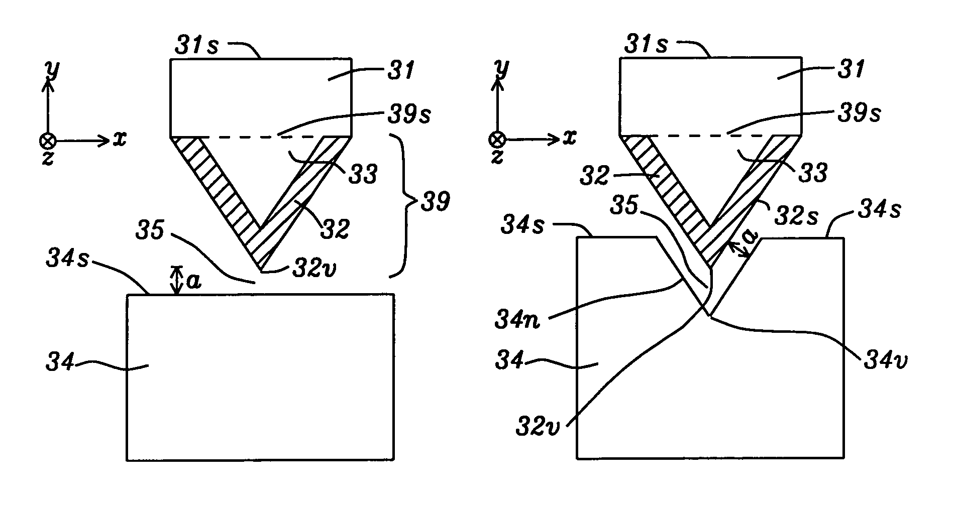
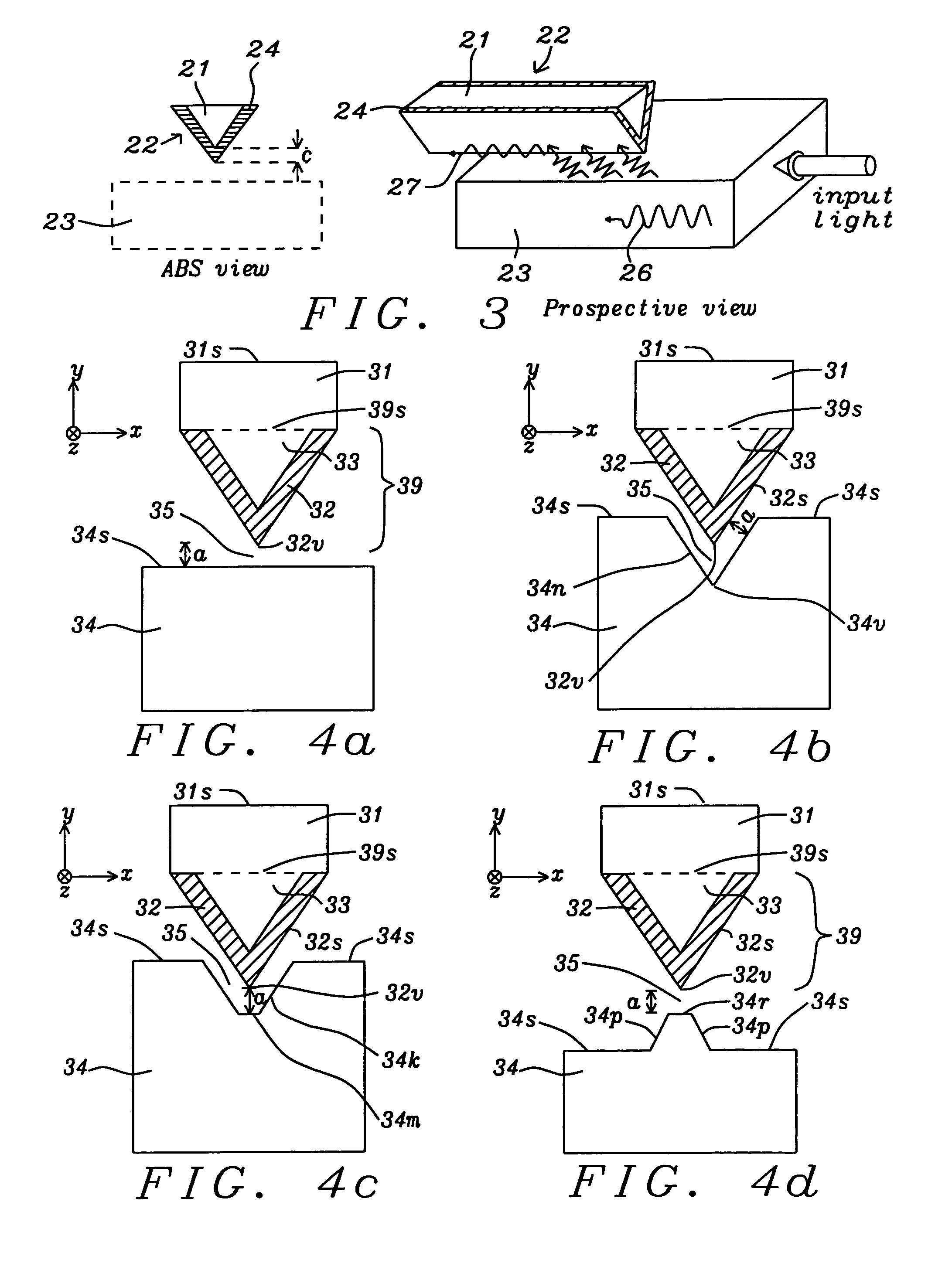
[0038]Referring to FIG. 4a, plasmon shield 34 has a surface 34s that is essentially parallel to trailing side 31s and faces vertex 32v according to one embodiment of the present invention. There is a dielectric layer (not shown) adjoining EPG 32 and planar surface 34s that separates the plasmon shield 34 from vertex 32v. The space (gap) 35 between the substantially planar surface 34s and vertex 32v has a preferred dimension a from 5 to 50 nm and may be tuned to achieve the desired optical spot size and shape on the magnetic medium (not shown). If the gap distance is 32v but is undesirably squeezed off to the sides of the tip. For gap distances >50 nm, the capability and advantage of the plasmon shield 34 to reduce the optical spot size is substantially lost. Note that the topography of surface 34s may be modified to optimize the optical spot shape. However, the first embodiment offers an advantage in terms of ease of manufacture.

[0039]In an alternative embodiment shown in FIG. 4b, a...

third embodiment

[0040]Referring to FIG. 4c, a third embodiment is depicted wherein the trench described in the previous embodiment may be modified to have a trapezoidal shape. In this case, a portion of plasmon shield 34 opposite vertex 32v is removed to form a surface 34s that is interrupted by a trench with two sloped sidewalls 34k that connect to a bottom trench section 34m which is essentially parallel to surface 34s in a z-axis direction. In one aspect, sidewalls 34k may be substantially parallel to sides 32s of EPG 32 and there is a gap distance a between vertex 32v and bottom 34m. Gap 35 as in previous embodiments is filled with a dielectric layer (not shown).

[0041]The dielectric gap 35 between EPG 32 and plasmon shield 34 may be tuned in terms of size for the desired optical spot shape in order to have a straight magnetic transition when aligning the magnetic field, and for the desired optical spot size reduction depending on tip radius. The present invention anticipates that the dielectric...

fourth embodiment

[0048]FIG. 5d is a plasmon shield / leading shield design that represents a modification of FIG. 4d wherein the leading shield 36 adjoins a section of the plasmon shield 34 opposite surface 34s. Preferably, the plasmon shield conforms to a top surface of leading shield 36 that includes surface 36s, sides 36p, and side 36r thereby providing a so-called convex shaped design for the plasmon shield and adjoining leading shield. Each of the two top surface sections 34p is substantially parallel to an underlying side 36p, and side 34r is aligned above surface section 36r in a y-axis direction. Top surface sections 36s of leading shield 36 are parallel to surface 34s and connect with side 36r through a side 36p. As a result, sides 36r, 36p form a protrusion on leading shield 36 wherein the side 36p is aligned parallel to vertex 32v in a z-axis direction, and below vertex 32v in a down-track direction along the y-axis.


PUM

PropertyMeasurementUnit
sizeaaaaaaaaaa
sizeaaaaaaaaaa
sizeaaaaaaaaaa

Abstract

A TAMR head is disclosed with a triangular shaped plasmon antenna covered on two sides with a plasmon layer that generates an edge plasmon mode along a vertex of the two plasmon sides formed opposite a main pole layer. A plasmon shield (PS) is formed along the ABS and opposite the vertex to confine an electric field from the edge plasmon mode within a small radius of the edge plasmon tip thereby reducing the optical spot size on the magnetic medium and enhancing writability. An end of a waveguide used to direct input electromagnetic radiation to the plasmon antenna adjoins a PS side opposite the ABS. In one embodiment, a magnetic shield may be formed along the ABS and adjoins the PS so that a first PS section terminates at the ABS and faces the vertex while a second PS section is formed between the magnetic shield and waveguide end.

Description

RELATED PATENT APPLICATION[0001]This application is related to the following: Ser. No. 12 / 456,290, filing date Jun. 15, 2009; assigned to a common assignee and herein incorporated by reference in its entirety.FIELD OF THE INVENTION[0002]The invention relates to magnetic read / write heads based on thermally assisted magnetic recording (TAMR) and in particular to a structure in which a plasmon antenna (PA) is included with a plasmon shield to enable the transfer of thermal energy with a small spot size at the media for higher recording density.BACKGROUND OF THE INVENTION[0003]TAMR is expected to be one of the future generation of magnetic recording technologies that will enable recording at ˜1-10 Tb / in2 data densities. TAMR involves raising the temperature of a small region of the magnetic medium to near its Curie temperature where both of its coercivity and anisotropy are significantly reduced and magnetic writing becomes easier to achieve even with weak write fields characteristic of...

Claims


Application Information

Patent Timeline
Patent Type & Authority Patents(United States)
IPC IPC(8): G11B11/00
CPCG02B6/107G11B5/314G11B2005/0021
Inventor JIN, XUHUIZHOU, YUCHENSMYTH, JOEMALETZKY, TOBIASTAKANO, KENICHISCHRECK, ERHARD
Owner HEADWAY TECH INC
Why Eureka
Try Eureka