

Method for fabricating semiconductor device
a semiconductor device and contact plug technology, applied in the direction of semiconductor devices, basic electric elements, electrical equipment, etc., can solve the problems of excessive reduction of the sectional area of the snc, and high external resistance (rext) of the semiconductor device, so as to reduce the external resistance of the semiconductor device
- Summary
- Abstract
- Description
- Claims
- Application Information
AI Technical Summary
Benefits of technology
Problems solved by technology
Method used
Image

Examples
first embodiment
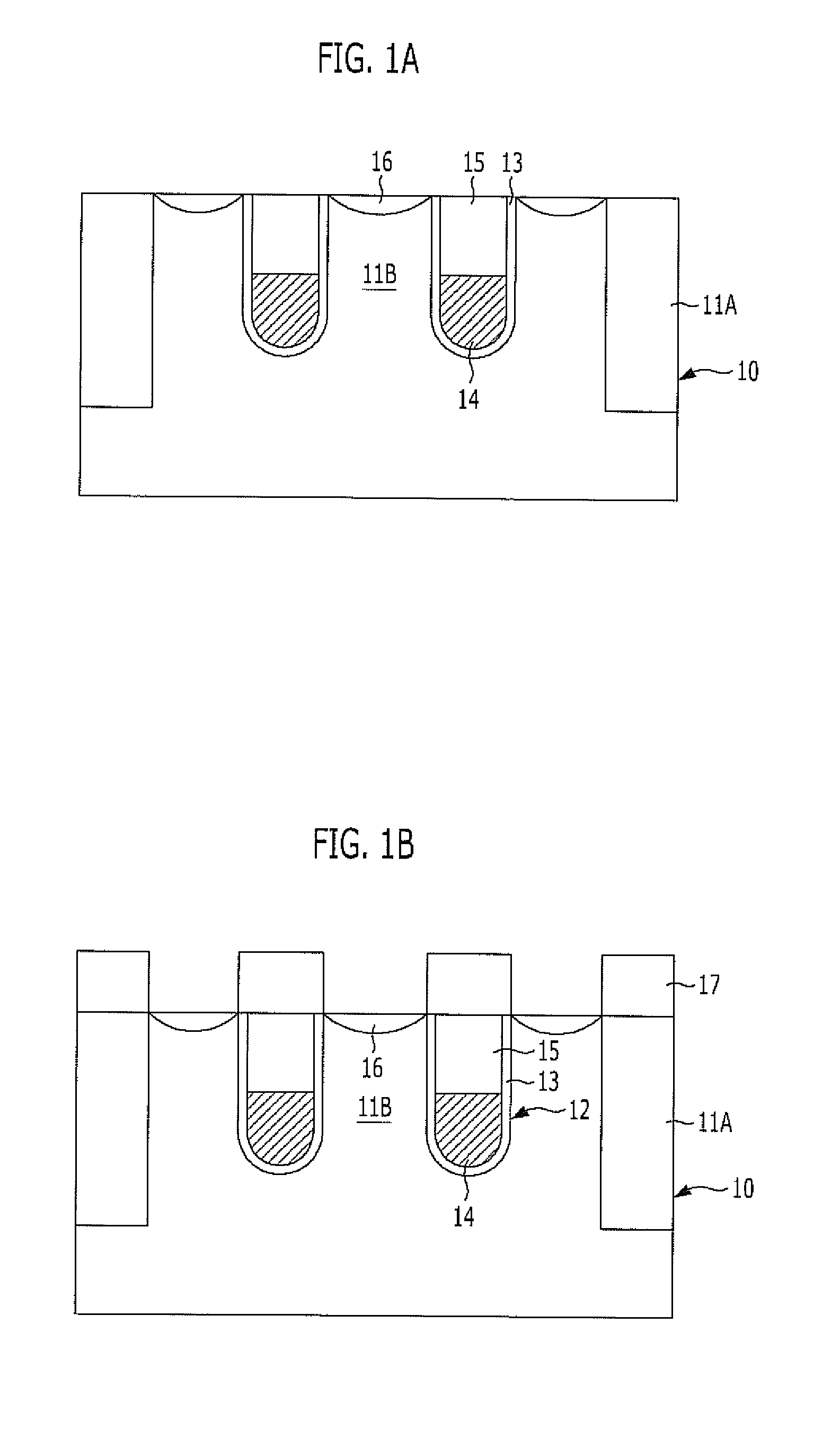
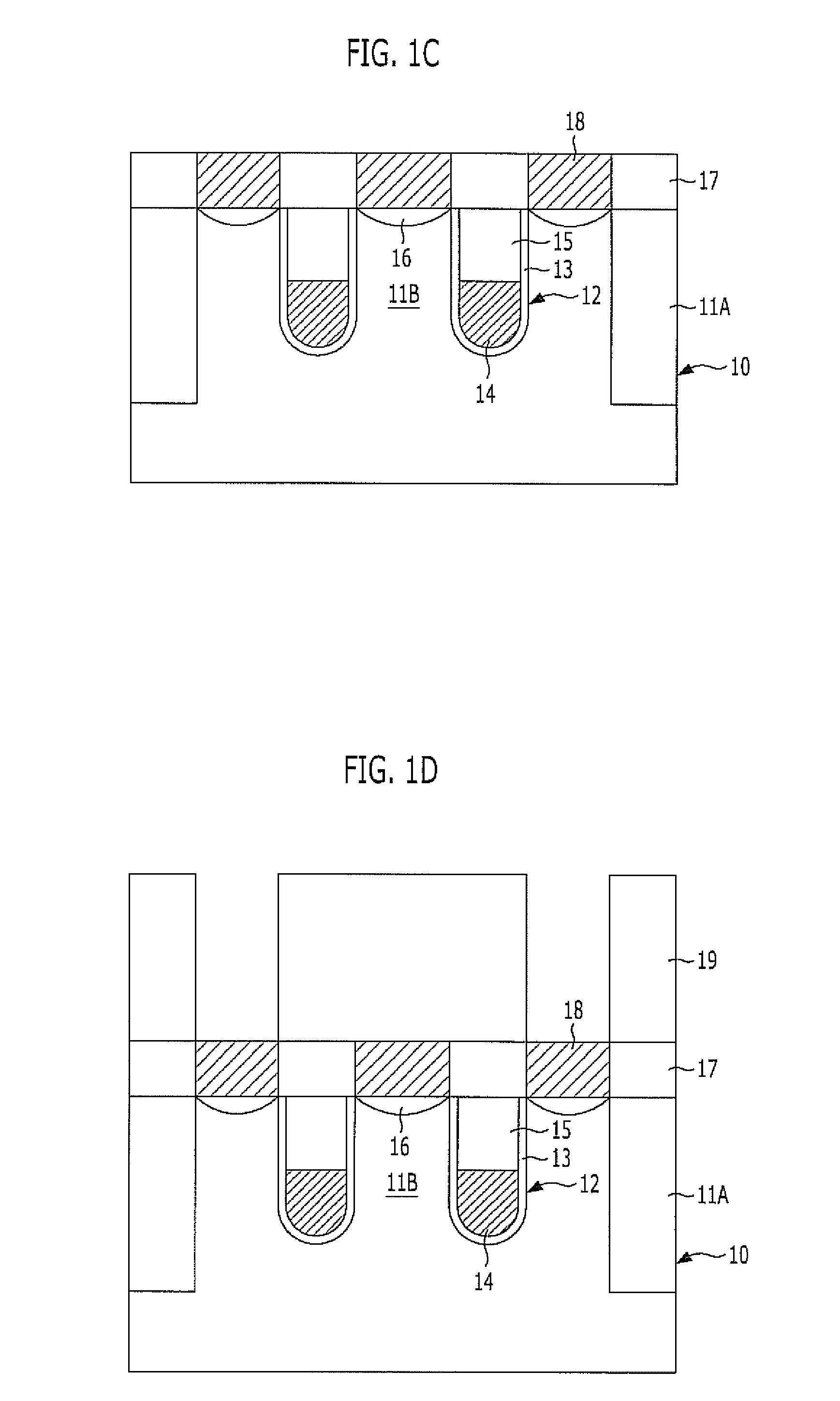
[0015]FIGS. 1A to 1F are cross-sectional views explaining a method for fabricating a semiconductor device in accordance with a first embodiment of the present invention.
[0016]Referring to FIG. 1A, an isolation layer 11A is formed on a substrate 10 through a shallow trench isolation (STI) process. The isolation layer 11A may include an oxide layer such as a high density plasma (HDP) oxide layer or a spin on dielectric (SOD) layer. An active area 11B is defined by the isolation layer 11A.
[0017]A buried gate 14 is formed in the substrate 10. More specifically, the buried gate 14 may be formed by the following process. First, the substrate 10 is etched to a desired depth to form a trench 12. The trench 12 is used for forming the buried gate 14. A mask pattern for opening a buried-gate area is formed over the substrate 10, and the substrate 10 is etched by using the mask pattern as an etching barrier to form the trench 12. As the mask pattern, a mask pattern used for forming the isolatio...
second embodiment
[0043]FIGS. 2A to 2F are cross-sectional views explaining a method for fabricating a semiconductor device in accordance with a second embodiment of the present invention.
[0044]Referring to FIG. 2A, an isolation layer 31A is formed on a substrate 30 through an STI process. The isolation layer 31A may include an oxide layer such as an HDP oxide layer or a SOD layer. An active area 31B is defined by the isolation layer 31A.
[0045]A buried gate 34 is formed in the substrate 30. More specifically, the buried gate 34 is formed by the following process. First, the substrate 30 is etched to a desired depth to form a trench 32. The trench 32 is used for forming the buried gate 34. A mask pattern for opening a buried-gate area is formed over the substrate 30, and the trench 32 is formed by etching the substrate 30 using the mask pattern as an etching barrier. As the mask pattern, a mask pattern used for forming the isolation layer 31A may be used as it is.
[0046]A gate dielectric layer 33 is fo...
third embodiment
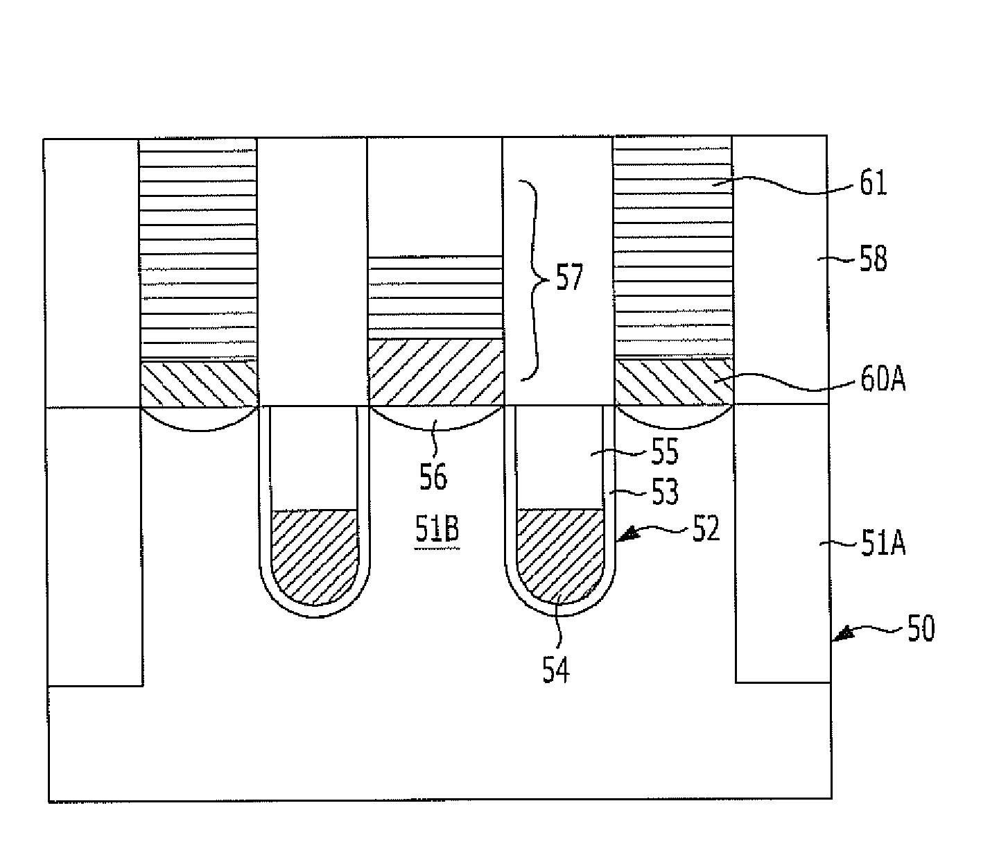
[0069]FIGS. 3A to 3E are cross-sectional views explaining a method for fabricating a semiconductor device in accordance with a third embodiment of the present invention.
[0070]Referring to FIG. 3A, an isolation layer 51A is formed on a substrate 50 through an STI process. The isolation layer 51A may include an oxide layer such as a HDP oxide layer or a SOD layer. An active area 51B is defined by the isolation layer 51A.
[0071]A buried gate 54 is formed in the substrate 50. More specifically, the buried gate 54 is formed by the following process. First, the substrate 50 is etched to a desired depth to form a trench 52. The trench 52 is used for forming the buried gate 54. A mask pattern for opening a buried-gate area is formed over the substrate 50, and the trench 52 is formed by etching the substrate 50 using the mask pattern as an etching barrier. As the mask pattern, a mask pattern used for forming the isolation layer 51A may be used as it is.
[0072]A gate dielectric layer 53 is form...
PUM
 Abstract
Description
Claims
Application Information