Reduced inductance IC leaded package

a technology of inductance reduction and lead package, which is applied in the direction of semiconductor/solid-state device details, semiconductor devices, electrical apparatus, etc., can solve the problems of affecting the normal function of the device, affecting the progress of semiconductor technology, and corrupting the electrical signal traveling through the device, so as to reduce crosstalk and reduce the effect of inductive coupling and less inductive coupling

Active Publication Date: 2011-12-13
ALTERA CORP
View PDF7 Cites 3 Cited by
  • Summary
  • Abstract
  • Description
  • Claims
  • Application Information

AI Technical Summary

Benefits of technology

[0011]The conductive sheet is arranged such that the path of a return current from the die to a lead finger at a high operating frequency, e.g., 300 MHz and above, concentrates at one portion on the sheet that is adjacent and parallel to the lead finger. As a result, in the present invention, there is more inductive coupling between a lead finger and the sheet and less inductive coupling between two immediately adjacent lead fingers. This substantially reduces the crosstalk caused by mutual inductance.
[0012]In addition, the conductive sheet is provided with a sufficient opening or openings to allow the encapsulant to flow through the sheet and form into one body. Such arrangement can effectively prevent detachment between the encapsulant and the conductive sheet during the packaging process.

Problems solved by technology

The downside of the aforementioned technology revolution is that certain previously ignored issues that are related to either a device or an electrical package protecting the device are becoming so critical that they may substantially hinder the progress of semiconductor technology if not dealt with appropriately.
If such noise is great enough, it may corrupt the electrical signal traveling through a device and disturb the normal function of the device.
Such an ideal scenario rarely exists in real life because it always takes some time for the voltage level to rise or drop from one extreme to another extreme.
Such a lower voltage level may cause the circuit to malfunction and produce undesirable results.
Higher frequency usually results in more significant crosstalk.
As a result, both of the two development trends discussed above exacerbate crosstalk-related problems.
While lower signal voltage is welcome because it reduces a device's power consumption, it unfortunately reduces the device's tolerance threshold for crosstalk at the same time.
Therefore, the crosstalk that previously could be safely ignored may pose a significant challenge to a device's normal operation now and therefore should be treated appropriately.

Method used


Image

  • Reduced inductance IC leaded package
  • Reduced inductance IC leaded package
  • Reduced inductance IC leaded package

Examples


Embodiment Construction

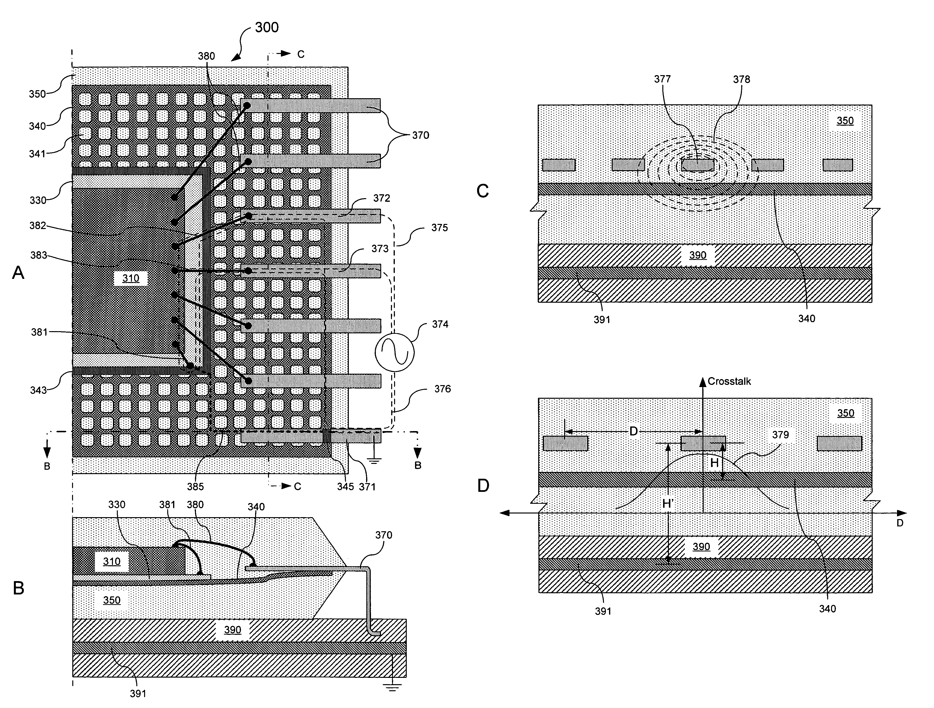
[0022]The present invention relates to a novel packaging strategy that can substantially reduce crosstalk caused by mutual inductance in an electrical device package, e.g., a quad flat package, and improve signal integrity of the electrical device embedded in the package.

[0023]Since crosstalk in an electrical device package largely depends upon the package's physical structure, e.g., distance of adjacent conductive paths, it is important to understand those structural features of the package that contribute to the creation of crosstalk.

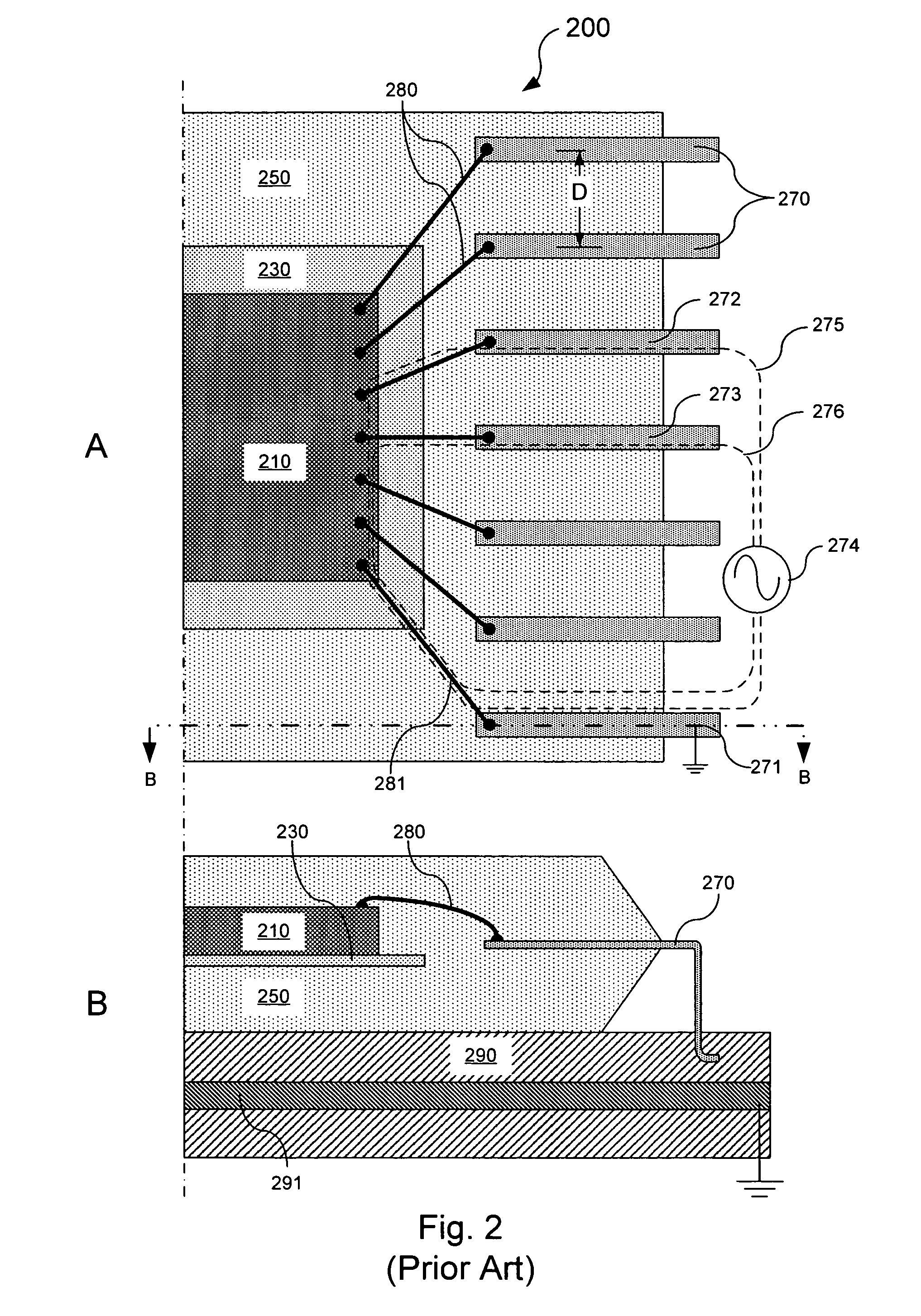
[0024]FIG. 2A is a top view of half of a prior art quad flat package 200. Package 200 comprises a semiconductor die 210, a die attach pad 230 below die 210 and encapsulant 250 surrounding die 210 and die attach pad 230. One end of each of a plurality of bondwires 280 is electrically connected to a bond pad on die 210 and the other end to a lead finger 270 deployed on an edge of package 200. Typically, there are lead fingers (not shown) on all the othe...


PUM


Abstract

The present invention is directed a novel method and apparatus for reducing crosstalk in a lead frame based electrical device package. One cause of the crosstalk in the lead frame package is the mutual inductance between adjacent lead fingers. A conductive sheet or mesh is introduced into the lead frame package such that one edge of the conductive sheet is below the die attach pad and electrically connected to the die and another edge is below the lead fingers and electrically connected to the ground lead of the package. Such arrangement significantly reduces the inductive coupling between adjacent lead fingers by coupling the lead fingers with the conductive sheet. The conductive sheet includes an array of through holes allowing the encapsulant material from the two sides of the sheet to flow smoothly together into one body.

Description

FIELD OF THE INVENTION[0001]The present invention relates generally to the field of electrical device packaging, and in particular to a lead package that significantly reduces self and mutual inductance of the package leads by introducing a voltage reference plane into the package.BACKGROUND OF THE INVENTION[0002]Semiconductor technology development has been following two significant trends from its very beginning. One trend is that the operating frequency of an integrated circuit (IC) device gets higher and higher. For example, the main operating frequency of the Intel386™ central processing unit (CPU) developed in the mid-1980's was only about 33 MHz. In contrast, the main operating frequency of today's Intel Pentium4™ CPU reaches 3.2 GHz, which is approximately 100 times faster than Intel386™ CPU. Higher frequency makes it possible for a device to process more data within a limited time period.[0003]The other trend is that the number of transistors per IC grows exponentially acco...

Claims


Application Information

Patent Timeline
Patent Type & Authority Patents(United States)
IPC IPC(8): H01L23/495
CPCH01L23/495H01L2223/6605H01L2224/48247H01L2224/48257H01L24/48H01L2924/10253H01L2924/3011H01L2924/30107H01L2924/00H01L24/49H01L2224/49109H01L2224/49171H01L2924/00014H01L2924/14H01L2924/181H01L2924/00012H01L2224/45099H01L2224/45015H01L2924/207
Inventor LONG, JON M.
Owner ALTERA CORP
Why Eureka
Try Eureka