Unlock instant, AI-driven research and patent intelligence for your innovation.

Non-volatile semiconductor memory device

a semiconductor memory and non-volatile technology, applied in static storage, digital storage, instruments, etc., can solve the problems of increasing the possibility of an over-program condition, reducing the data retention characteristics, and high write speed

Inactive Publication Date: 2011-12-20
KK TOSHIBA
View PDF30 Cites 13 Cited by
  • Summary
  • Abstract
  • Description
  • Claims
  • Application Information

AI Technical Summary

Benefits of technology

This solution allows for effective judgment and management of degraded memory blocks, preventing over-program conditions, improving data retention, and reducing the time required for write operations while enhancing data reliability.

Problems solved by technology

With a higher threshold voltage, the degraded memory cell transistor will have a higher write speed, thus increasing the possibility of an over-program condition (failure of being biased above a desired threshold voltage as a result of writing).
Further, with the trapped electrons detrapped by being left at a high temperature, the degraded memory cell transistor is biased far below the threshold voltage, and thereby decreases in data retention characteristics.
It is therefore very difficult to monitor reliability quickly during process change or commercial production.

Method used


Image

  • Non-volatile semiconductor memory device
  • Non-volatile semiconductor memory device
  • Non-volatile semiconductor memory device

Examples


first embodiment

[0035][1. Configuration of Memory System 1]

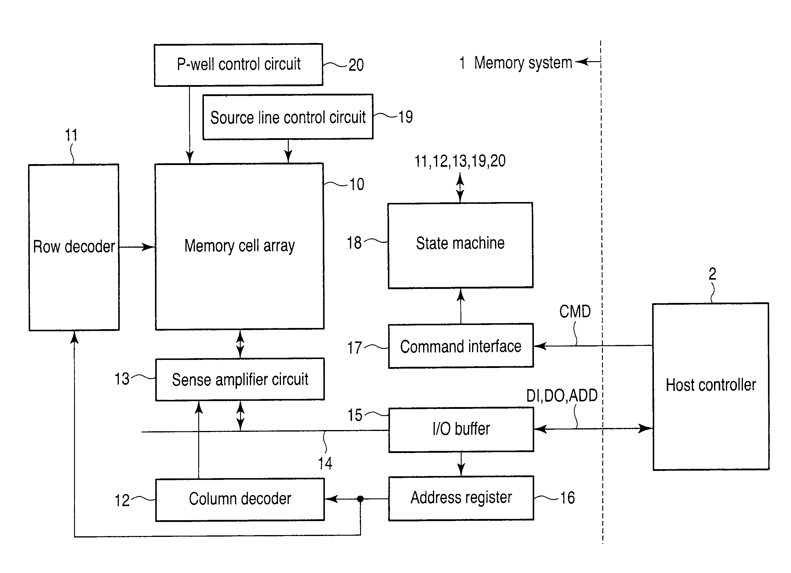
[0036]A memory system (non-volatile semiconductor memory device) 1 of the present embodiment is mounted on a printed substrate, for example, on which a host device is mounted, and transfers data to / from the host device via a bus. Alternatively, the memory system 1 of the present invention is configured to be detachable from the host device, and transfers data to / from the host device via a bus in a state of being connected to the host device. FIG. 1 is a block diagram showing a configuration of the memory system 1 according to the first embodiment.

[0037]A memory cell array 10 can be electrically rewritten, and is formed of a NAND flash memory, which is a type of non-volatile semiconductor memory. The memory cell array 10 comprises a plurality of blocks, each of which forms a unit of data erasure. The memory cell array 10 is provided with a plurality of word lines WL each extending in a row direction. Further, the memory cell array 10 is prov...

second embodiment

[0101]The blocks are collectively erased prior to writing. The erasure operation will be performed as follows. First, all the word lines in the blocks are set to the ground voltage Vss by the row decoder 11. Second, the P-well control circuit 20 applies an erasure voltage Vera of approximately 20V to the P-well 31 in which the blocks are formed. Thereby, all the memory cell transistors MT in the blocks are brought into an erasure state in which the threshold voltage is low, after the electrons in the floating gate electrode are emitted to the P-well 31. The data erasure is performed by repetition of application of an erasure voltage and erasure verification confirming the state of erasure.

[0102]In the second embodiment, an erasure verification operation for judging whether the data has been correctly erased is applied to measure the cell current of the memory cell transistor MT. FIG. 12 is a timing chart showing a cell current measurement operation of the memory system 1 according t...

third embodiment

[0111]A degraded memory cell transistor is more difficult to erase than a not-yet-degraded memory cell, since the threshold voltage of the memory cell transistor becomes high due to an increase in electrons trapped in the tunnel insulation film. In the third embodiment, whether the block has been degraded or not is judged prior to an erasure operation, and an erasure operation is performed on the degraded block with a higher erasure voltage. FIG. 13 is a flowchart showing an erasure operation of a memory system 1 according to a third embodiment.

[0112]A state machine 18 reads a flag indicative of whether a block to be erased has been degraded or not from the block (step S30). Then, the state machine 18 uses the flag to judge whether the block has been degraded or not (step S31). If the block has not been degraded, a P-well control circuit 20 uses a normal erasure voltage to erase data in the block to be erased (step S33).

[0113]When the block is judged as having been degraded in step ...


PUM


Abstract

A non-volatile semiconductor memory device includes a non-volatile memory having a plurality of blocks each including a plurality of memory cells, a bit line electrically connected to one end of a current path of the memory cell, a source line electrically connected to the other end of the current path of the memory cell, a word line electrically connected to the gate electrode, a sense amplifier circuit electrically connected to the bit line and configured to read data from the memory cell, a row decoder electrically connected to the word line and configured to apply a read voltage at which the memory cell is set to an ON state to the word line, and a controller configured to measure a cell current flowing through the memory cell in the ON state to judge whether the memory cell has been degraded.

Description

CROSS-REFERENCE TO RELATED APPLICATIONS[0001]This application is based upon and claims the benefit of priority from prior Japanese Patent Application No. 2008-117729, filed Apr. 28, 2008, the entire contents of which are incorporated herein by reference.BACKGROUND OF THE INVENTION[0002]1. Field of the Invention[0003]The present invention relates to a non-volatile semiconductor memory device including, for example, a non-volatile semiconductor memory device which can be electrically rewritten.[0004]2. Description of the Related Art[0005]As a non-volatile semiconductor memory which can be electrically rewritten, a NAND flash memory is known. The NAND flash memory comprises a memory cell transistor having a stacked gate structure in which a tunnel insulation film, a charge storage layer, an intergate insulation film, and a control gate electrode are sequentially stacked on a semiconductor substrate.[0006]With this structure, the memory cell transistor may be degraded by an increase in ...

Claims


Application Information

Patent Timeline
Patent Type & Authority Patents(United States)
IPC IPC(8): G11C11/34
CPCG11C11/5635G11C11/5642G11C16/0483G11C16/349G11C29/028G11C29/50G11C29/82G11C16/04G11C2029/5006G11C2211/565
Inventor UENO, KOKINAGASHIMA, HIROYUKI
Owner KK TOSHIBA