Phononic crystal devices

a phononic crystal and crystal device technology, applied in the field of phononic crystal devices, can solve problems such as frequency gaps opening, and achieve the effects of low thermal conductivity, and improved thermal conductivity and heat capacity

US8094023B1Active Publication Date: 2012-01-10NAT TECH & ENG SOLUTIONS OF SANDIA LLC
9 Cites 78 Cited by

Patent Information

Authority / Receiving Office
US · United States
Current Assignee / Owner
Publication Date
2012-01-10

Smart Images

  • Figure 1
    Figure 1
  • Figure 2
    Figure 2
  • Figure 3
    Figure 3
Patent Text Reader

Abstract

Phononic crystals that have the ability to modify and control the thermal black body phonon distribution and the phonon component of heat transport in a solid. In particular, the thermal conductivity and heat capacity can be modified by altering the phonon density of states in a phononic crystal. The present invention is directed to phononic crystal devices and materials such as radio frequency (RF) tags powered from ambient heat, dielectrics with extremely low thermal conductivity, thermoelectric materials with a higher ratio of electrical-to-thermal conductivity, materials with phononically engineered heat capacity, phononic crystal waveguides that enable accelerated cooling, and a variety of low temperature application devices.
Need to check novelty before this filing date? Find Prior Art

Description

CROSS-REFERENCE TO RELATED APPLICATION

[0001] This application claims the benefit of U.S. Provisional Application No. 61 / 035,148, filed Mar. 10, 2008, which is incorporated herein by reference.STATEMENT OF GOVERNMENT INTEREST

[0002] This invention was made with Government support under contract no. DE-AC04-94AL85000 awarded by the U.S. Department of Energy to Sandia Corporation. The Government has certain rights in the invention.FIELD OF THE INVENTION

[0003] The present invention relates to phononic crystals and, in particular, to nano-scale phononic crystals that can be used for thermal management and noise mitigation in devices.BACKGROUND OF THE INVENTION

[0004] An acoustic or phononic bandgap is the phononic analog of a photonic bandgap, wherein a range of acoustic frequencies are forbidden to exist in a structured material. Phononic bandgaps are realized by embedding periodic scatterers in a homogeneous host matrix that propagates an acoustic wave. The scatterer material has a density a...

Examples

Embodiment Construction

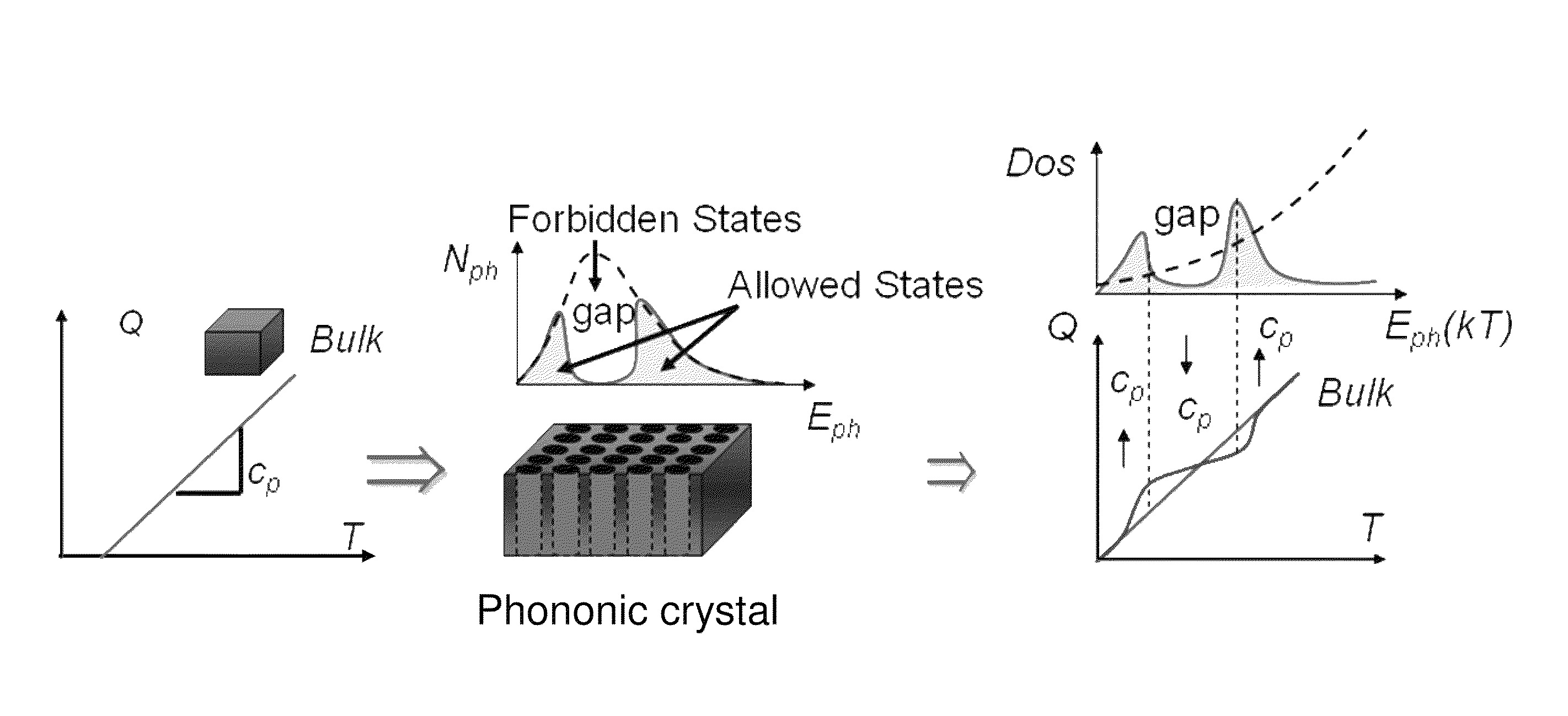
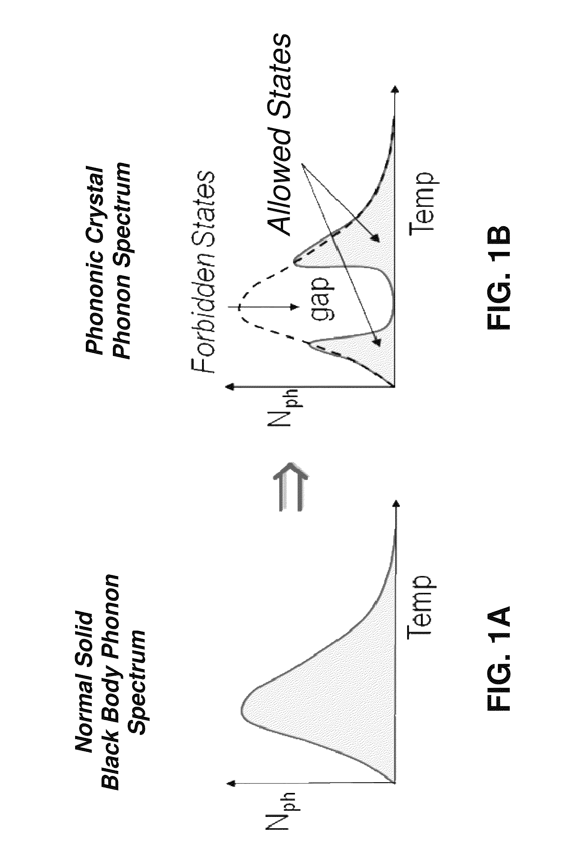
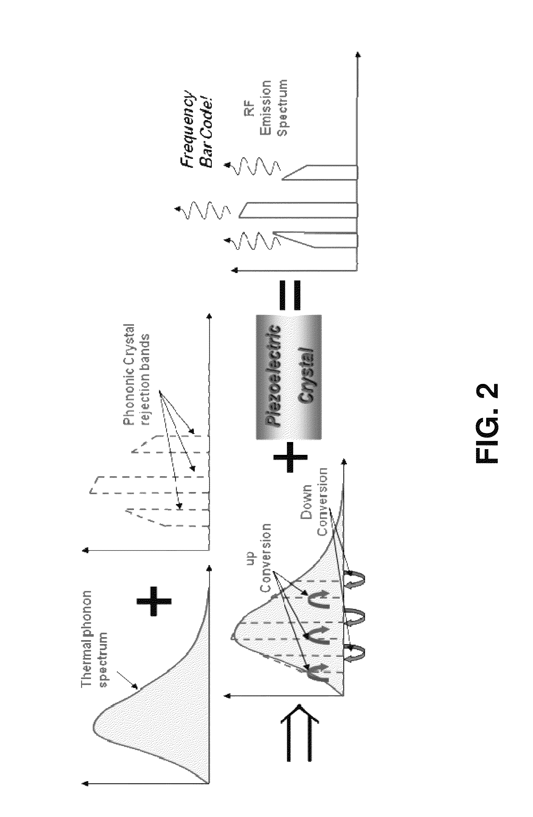
[0020]Shown in FIG. 1A is the black body phonon distribution in a conventional solid material versus temperature. By altering the structure of the material to form a phononic crystal, a phononic bandgap can be realized in the material, as shown in FIG. 1B. This phononic bandgap forbids the existence of phonons in the material over a wide range of frequencies or equivalent temperatures and redistributes the thermally induced black body phonon spectrum in the material. Therefore, the thermal phonon distribution can be molded and shaped by artificially changing the density of states of the phononic crystal. Such phononic crystals can provide dielectrics with reduced thermal conduction, thermopiles that can scavenge thermal energy, thermoelectric coolers, materials with good electrical but poor thermal conduction, and devices that can shield Johnson noise.

[0021]Phononic crystals are formed by the periodic arrangement of scattering centers in a host matrix with a high acoustic impedance ...