One-dimensional arrays of block copolymer cylinders and applications thereof

a technology of self-assembling and copolymer cylinders, which is applied in the direction of photomechanical equipment, instruments, and semiconductor/solid-state device details, etc., can solve the problems of poor etch mask structure, difficult optical lithographic processing methods to fabricate structures and features at the sub-30 nanometer level, and significant challenges to electrical contacts to conductive lines

Active Publication Date: 2012-01-24
MICRON TECH INC
View PDF195 Cites 61 Cited by
  • Summary
  • Abstract
  • Description
  • Claims
  • Application Information

AI Technical Summary

Problems solved by technology

Making electrical contacts to conductive lines has become a significant challenge as the dimensions of semiconductor features shrink to sizes that are not easily accessible by conventional lithography.
Optical lithographic processing methods have difficulty fabricating structures and features at the sub-30 nanometer level.
However, a 1-D array of spheres provides a poor etch mask structure where, even if the sphere material can be removed, there is little aspect ratio to the remaining porous film.

Method used


Image

  • One-dimensional arrays of block copolymer cylinders and applications thereof
  • One-dimensional arrays of block copolymer cylinders and applications thereof
  • One-dimensional arrays of block copolymer cylinders and applications thereof

Examples


Embodiment Construction

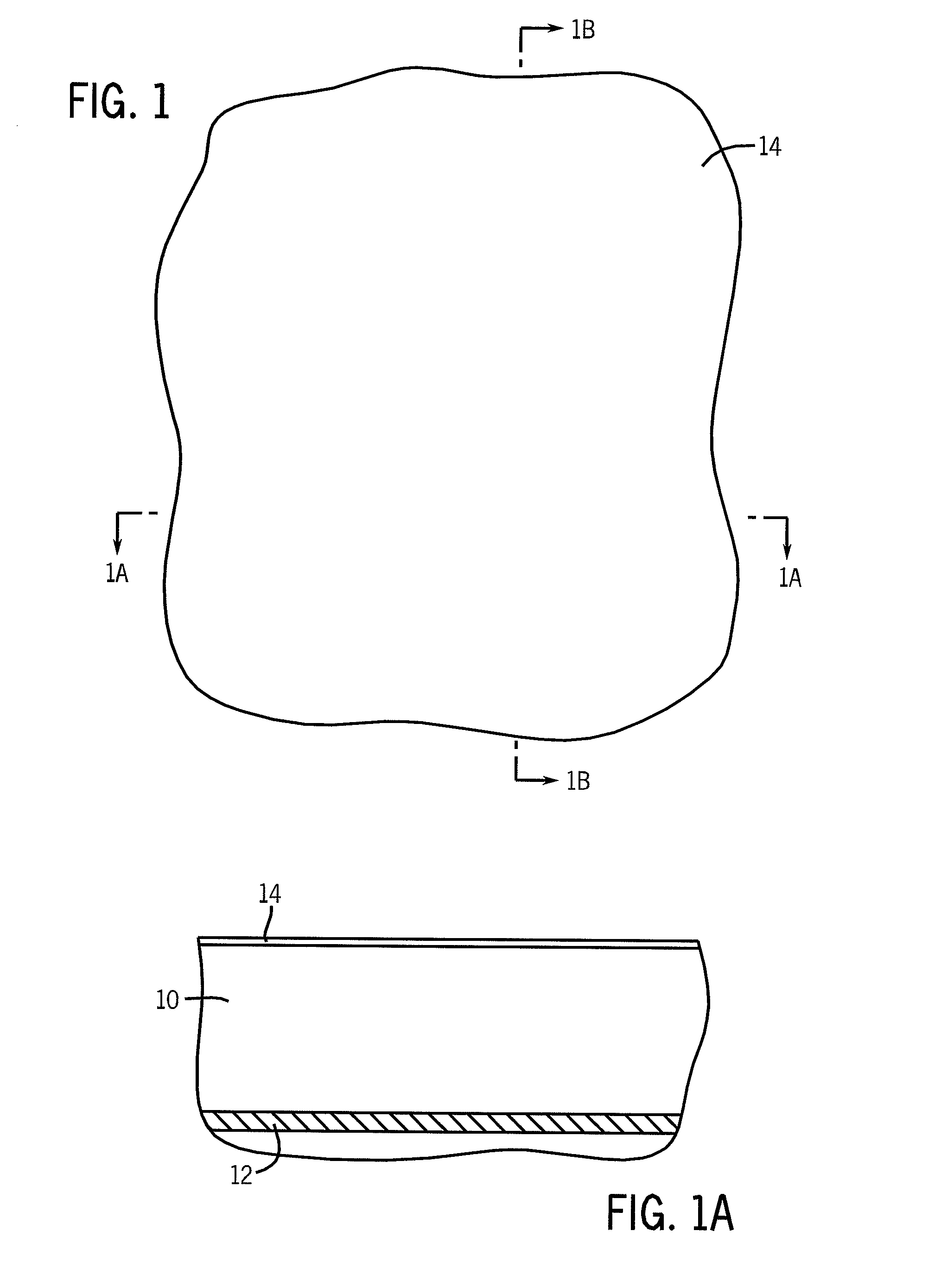
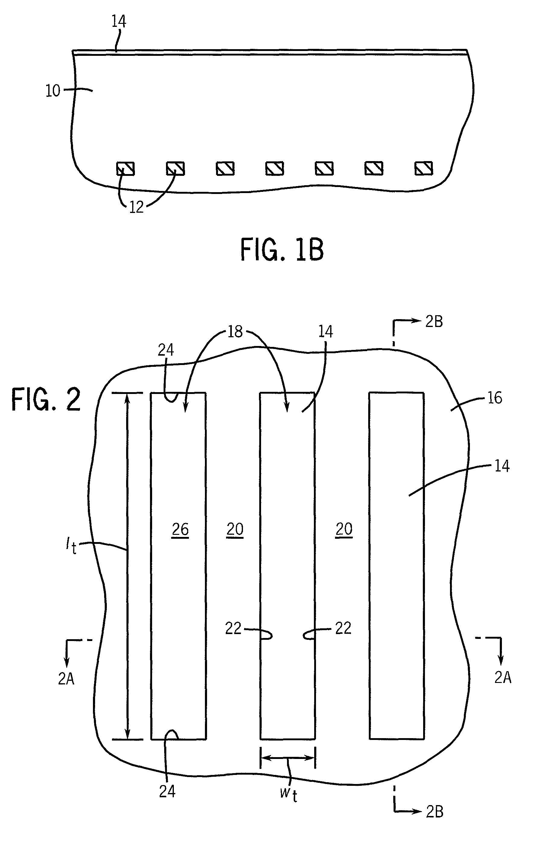
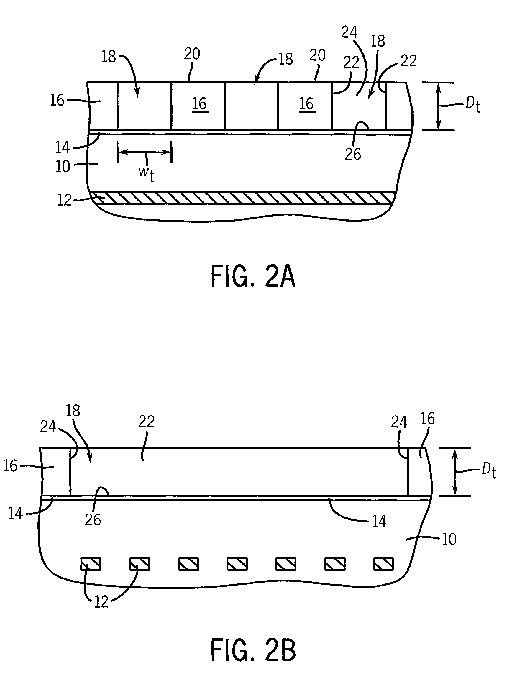
[0023]The following description with reference to the drawings provides illustrative examples of devices and methods according to embodiments of the invention. Such description is for illustrative purposes only and not for purposes of limiting the same.

[0024]In the context of the current application, the term “semiconductor substrate” or “semiconductive substrate” or “semiconductive wafer fragment” or “wafer fragment” or “wafer” will be understood to mean any construction comprising semiconductor material, including but not limited to bulk semiconductive materials such as a semiconductor wafer (either alone or in assemblies comprising other materials thereon), and semiconductive material layers (either alone or in assemblies comprising other materials). The term “substrate” refers to any supporting structure including, but not limited to, the semiconductive substrates, wafer fragments or wafers described above.

[0025]“Lo” as used herein is the inherent periodicity or pitch value (bul...


PUM


Abstract

Methods for fabricating sublithographic, nanoscale microstructures in one-dimensional arrays utilizing self-assembling block copolymers, and films and devices formed from these methods are provided.

Description

TECHNICAL FIELD[0001]Embodiments of the invention relate to methods of fabricating thin films of self-assembling block copolymers, and devices resulting from those methods.BACKGROUND OF THE INVENTION[0002]As the development of nanoscale mechanical, electrical, chemical and biological devices and systems increases, new processes and materials are needed to fabricate nanoscale devices and components. Making electrical contacts to conductive lines has become a significant challenge as the dimensions of semiconductor features shrink to sizes that are not easily accessible by conventional lithography. Optical lithographic processing methods have difficulty fabricating structures and features at the sub-30 nanometer level. The use of self assembling diblock copolymers presents another route to patterning at nanoscale dimensions. Diblock copolymer films spontaneously assembly into periodic structures by microphase separation of the constituent polymer blocks after annealing, for example by...

Claims


Application Information

Patent Timeline
Patent Type & Authority Patents(United States)
IPC IPC(8): B32B5/12
CPCB81C1/00031B82Y30/00H01L21/0337H01L21/0338H01L21/31144H01L21/76802Y10T428/24182Y10S977/778Y10S977/784Y10S977/789Y10S977/79Y10T428/24058Y10T428/24174Y10T428/24124B81C2201/0149G03F7/0002H01L21/76816
Inventor MILLWARD, DAN B.STUEN, KARL
Owner MICRON TECH INC
Why Eureka
Try Eureka