Method for manufacturing field-effect transistor

a field-effect transistor and manufacturing method technology, applied in the direction of basic electric elements, electrical apparatus, semiconductor devices, etc., can solve the problems of difficult to increase electron mobility, the inability of the zno-based compound to form a stable amorphous phase at room temperature, etc., to reduce parasitic resistance, increase the conductivity of the oxide semiconductor layer, and reduce the effect of parasitic resistan

Active Publication Date: 2012-02-07
CANON KK
View PDF22 Cites 98 Cited by
  • Summary
  • Abstract
  • Description
  • Claims
  • Application Information

AI Technical Summary

Benefits of technology

[0014]When annealing is performed in an atmosphere containing water, heavy water, steam or heavy water steam (hereinafter referred to as moisture), according to the method for manufacturing a field-effect transistor of the present invention, moisture passes through the insulating layer formed on the oxide semiconductor and diffuses in the oxide semiconductor layer. As a result, the conductivity of the oxide semiconductor layer can be increased.
[0015]In addition, when employing a structure which protects the channel regions of a field-effect transistor from a steam atmosphere, the conductivity in regions in contact with the source electrode and the drain electrode can be increased. This can reduce the parasitic resistance generated between the source electrode and the oxide semiconductor layer and between the drain electrode and the oxide semiconductor layer, and a field-effect transistor having excellent characteristics can be produced.

Problems solved by technology

However, a ZnO-based compound cannot form a stable amorphous phase at room temperature, but forms a polycrystalline phase.
It is therefore difficult to increase electron mobility because of scattering at grain boundaries.

Method used


Image

  • Method for manufacturing field-effect transistor
  • Method for manufacturing field-effect transistor
  • Method for manufacturing field-effect transistor

Examples


embodiment 1

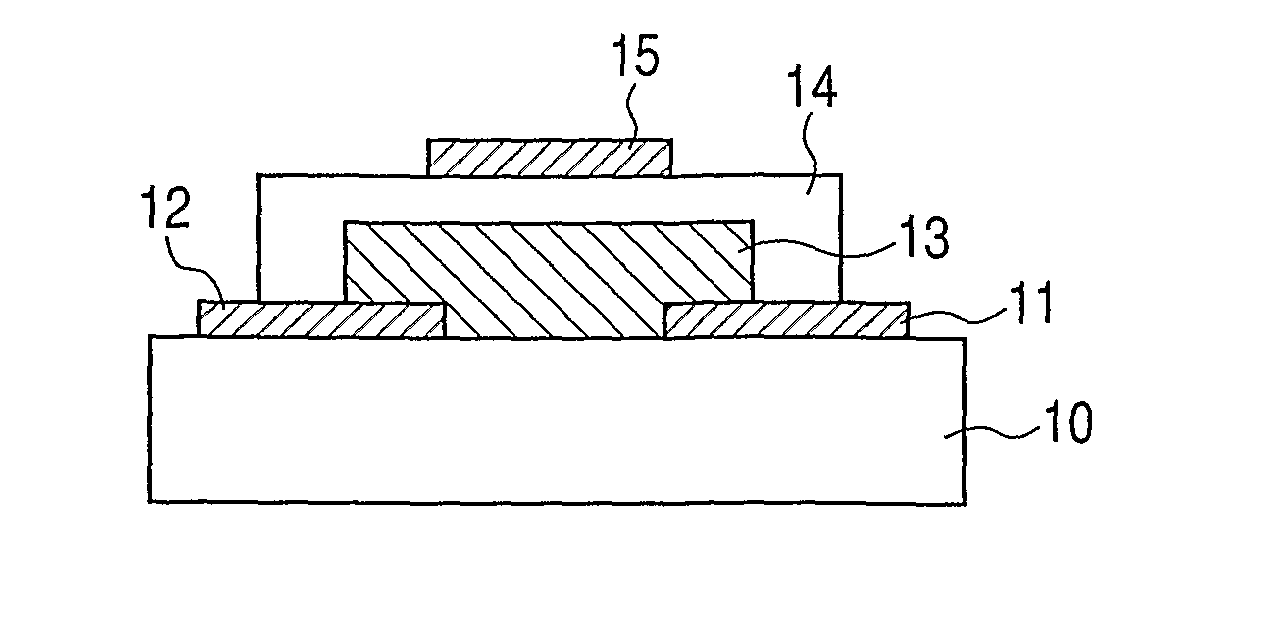
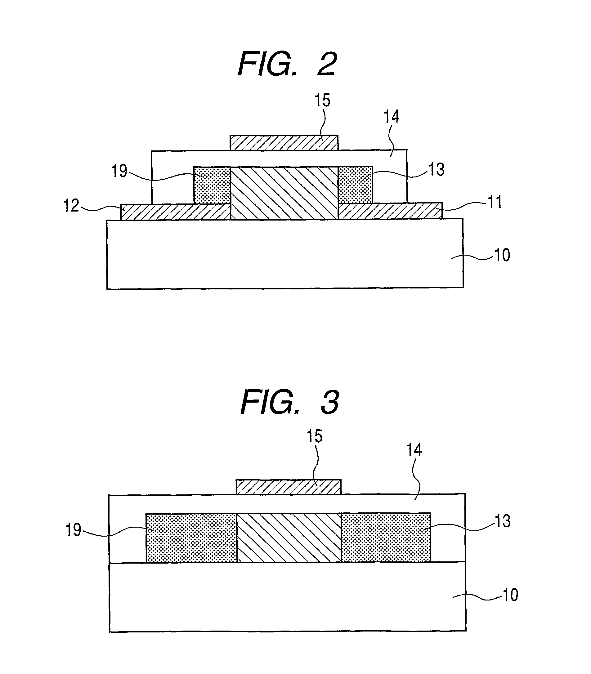
[0069]FIG. 1A illustrates a method for manufacturing a top-gate stagger field-effect transistor.

[0070]An electrode layer for forming a source electrode and a drain electrode is formed on a glass substrate 10 (1737, manufactured by Corning Inc.) by sputtering. The electrodes are formed of indium tin oxide (ITO) and have a thickness of 50 nm.

[0071]Then, the electrode layer is patterned by photolithography and etching to form the source electrode 11 and the drain electrode 12.

[0072]Next, an In—Zn—Ga—O oxide amorphous semiconductor layer 13 having a thickness of 30 nm is formed on the glass substrate 10 having the source electrode 11 and the drain electrode 12. The oxide semiconductor layer is formed with a radio frequency (RF) sputtering apparatus at a substrate temperature of room temperature (25° C.). A target is a three-inch polycrystalline sintered compact having an In2O3.ZnO composition. The RF input power is 200 W. The total pressure of the atmosphere when the film is formed is 0...

embodiment 2

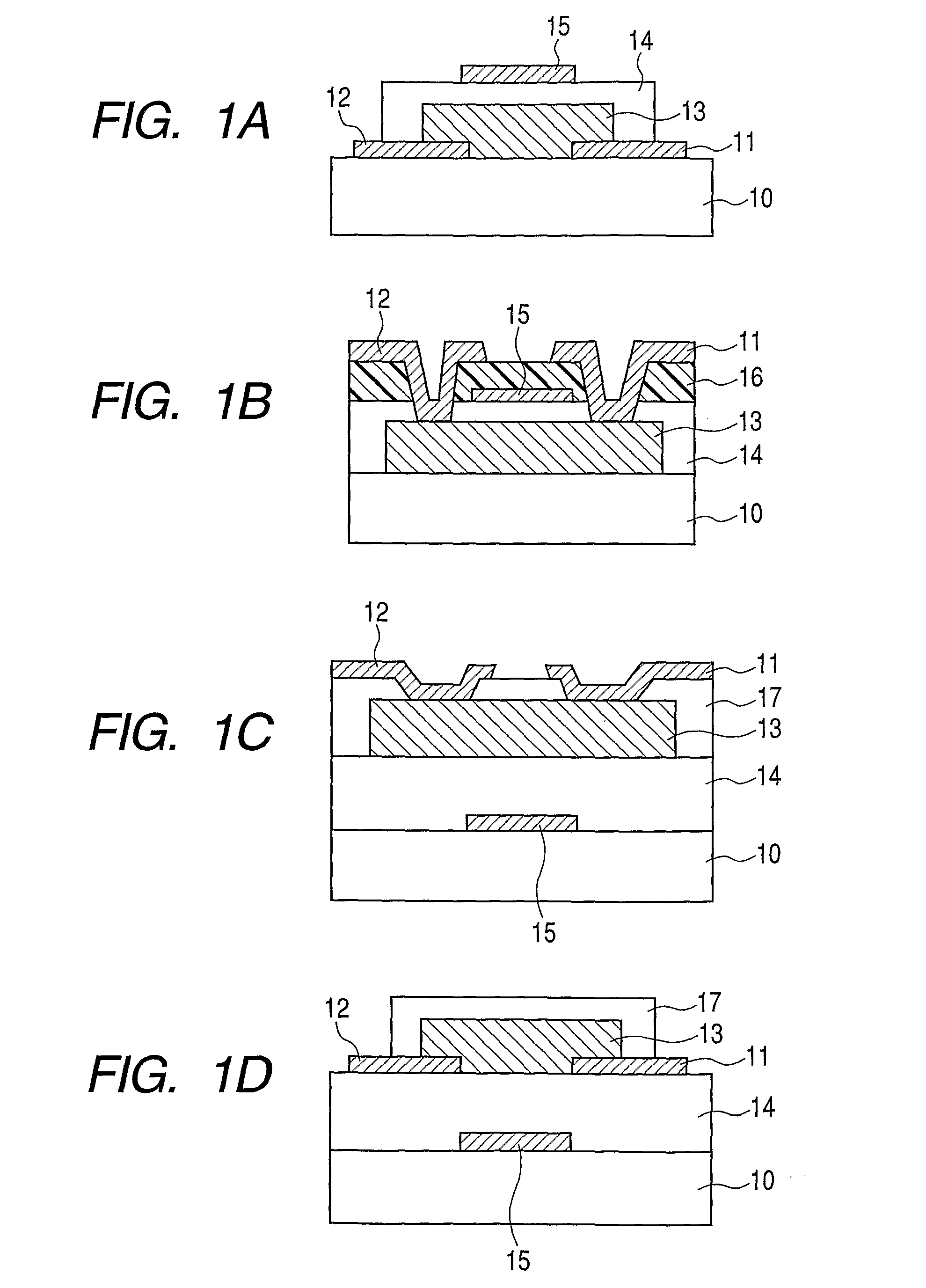
[0078]FIG. 1B illustrates a method for manufacturing a top-gate / top-contact field-effect transistor.

[0079]First, an In—Zn—Ga—O amorphous oxide semiconductor layer 13 is formed at a thickness of 50 nm on the glass substrate 10 (1737, manufactured by Corning Inc.) illustrated in FIG. 1B. The oxide semiconductor film is formed by an RF sputtering apparatus with the substrate temperature of room temperature (25° C.). A three-inch polycrystalline sintered compact having an In2O3.ZnO composition is used as the target, and the RF input power is 200 W. The total pressure of the atmosphere when the film is formed is 0.5 Pa, and the gas flow rate at that time is Ar:O2=93:7. After that, photolithography technology and etching technology are used to pattern the oxide semiconductor layer 13.

[0080]Next, the gate insulating layer 14 and a gate electrode 15 are formed.

[0081]The gate insulating layer 14 is formed of SiO2 as a target by sputtering and has a thickness of 100 nm. The gate insulating la...

embodiment 3

[0086]FIG. 1C illustrates a method for manufacturing a bottom-gate top-contact field-effect transistor.

[0087]First, the gate electrode 15 is patterned and formed on the substrate 10 (1737, manufactured by Corning Inc.) using photolithography technology and etching technology. The electrode is formed of Mo at a thickness of 50 nm on the glass substrate 10 by sputtering.

[0088]Next, with regard to the gate insulating layer 14, SiO2 is used as the target, and an SiO2 film with a thickness of 200 nm is formed by sputtering. Further, an In—Zn—Ga—O amorphous oxide semiconductor material with a thickness of 30 nm is used as the oxide semiconductor film 13.

[0089]The oxide semiconductor film is formed by using an RF sputtering apparatus with the substrate temperature of room temperature (25° C.). A three-inch polycrystalline sintered compact having an In2O3.ZnO composition is used as the target, and the RF input power is 200 W. The total pressure of the atmosphere when the film is formed is 0...


PUM

PropertyMeasurementUnit
pressureaaaaaaaaaa
thicknessaaaaaaaaaa
thicknessaaaaaaaaaa

Abstract

A method for manufacturing a field-effect transistor is provided. The field-effect transistor includes on a substrate a source electrode, a drain electrode, an oxide semiconductor layer, an insulating layer and a gate electrode. The method includes, after forming the insulating layer on the oxide semiconductor layer, an annealing step of increasing the electrical conductivity of the oxide semiconductor layers by annealing in an atmosphere containing moisture. The steam pressure at the annealing step is higher than the saturated vapor pressure in the atmosphere at the annealing temperature.

Description

TECHNICAL FIELD[0001]The present invention relates to a method for manufacturing a field-effect transistor. More particularly, the present invention relates to a method for manufacturing a field-effect transistor having an oxide film as a semiconductor layer.BACKGROUND ART[0002]In recent years, thin film transistors (TFTs) including a channel layer of a polycrystalline transparent conductive ZnO-based oxide thin film have actively been developed (Japanese Patent Application Laid-Open No. 2002-076356).[0003]Japanese Patent Application Laid-Open No. 2002-076356 states that because the thin film can be formed at low temperature and is transparent to visible light, a flexible transparent TFT can be formed on a substrate such as a plastic plate or a film.[0004]However, a ZnO-based compound cannot form a stable amorphous phase at room temperature, but forms a polycrystalline phase. It is therefore difficult to increase electron mobility because of scattering at grain boundaries. Furthermo...

Claims


Application Information

Patent Timeline
Patent Type & Authority Patents(United States)
IPC IPC(8): H01L21/00
CPCH01L29/78618H01L29/66969H01L29/4908H01L29/7869H01L29/66742H01L29/78606
Inventor HAYASHI, RYOYABUTA, HISATOTATEISHI, YOSHINORIKAJI, NOBUYUKI
Owner CANON KK
Why Eureka
Try Eureka