Bump structure formed from using removable mandrel

a technology of mandrel and bump, which is applied in the manufacture of printed circuits, printed circuit aspects, basic electric elements, etc., can solve the problems of difficult to raise the height of the bump, the thickness of the material which constitutes the plating resist is limited, and the height of the formed bump may disperse, etc., to achieve high aspect ratio and fine pitch

Inactive Publication Date: 2012-02-21
INVENSAS CORP
View PDF9 Cites 70 Cited by
  • Summary
  • Abstract
  • Description
  • Claims
  • Application Information

AI Technical Summary

Benefits of technology

[0013]The embodiments disclosed herein provide solutions to the problems of the related art and provide a process for forming a bump structure and the bump structure which can achieve a bump having a high aspect ratio. Even if a plurality of bumps is formed, dispersion of the height of the bumps is small and a fine pitch between the bumps can be achieved.
[0025]The bump-structure forming member may include a member in a state in which the metal layer formed in the bump-forming recess remains formed in the bump-forming recess without being removed from the bump-forming die body and the bump-forming die lid. For example, by distributing the members in this state through the market, a purchaser can form a wiring pattern on that member or overlay a circuit board. Removal of the bump-forming die body and the bump-forming die lid at a stage in which a desired processing is completed, a desired circuit board in which the bump structure is formed can be achieved. Because the bump-structure forming member is in the state in which the bump-forming die body and the bump-forming die lid are not removed, the bump-forming die body and the bump-forming die lid take a role of a supporting body, which is convenient for distribution as a product and subsequent processing.
[0031]Thus, there is no restriction by plating resist unlike the electric plating method using the plating resist. Further, because the above-mentioned process enables the height of the formed protrusion, that is, the height of the bump to be adjusted by changing the thickness of the bump-forming die body, the bump having a larger height than by a method by the electric plating using the plating resist or a method by etching can be formed. Because the diameter of the bump to be formed can be adjusted by changing the diameter of the opening of the bump-forming recess, a bump having a high aspect ratio can be formed.
[0032]If a plurality of the bumps is formed according to this process, the height of each bump is defined by the thickness of the bump-forming die body, thereby suppressing the dispersion of the height. Further, because there is no restriction by etching resist unlike by the method by etching, a fine pitch between the bumps can be achieved.

Problems solved by technology

However, when a plurality of bumps is formed according to the aforementioned method by electric plating using plating resist, the height of the formed bumps may disperse because metal is deposited within each opening of the plating resist.
However, there is a limitation in the thickness of material which constitutes the plating resist, such as DFR on market.
Thus, it is difficult to raise the height of the bump.
Additionally, the above-mentioned problem originating from the height of the plating resist never occurs.
Therefore, if it is desired to form a bump having a larger height with respect to the diameter of the bottom portion, that is, a bump having a high aspect ratio, the method by etching has a limitation.
Additionally, there is a limitation by the etching resist.
Therefore, the interval of the bumps, that is, the accuracy of a fine pitch is limited by the etching resist.

Method used


Image

  • Bump structure formed from using removable mandrel
  • Bump structure formed from using removable mandrel
  • Bump structure formed from using removable mandrel

Examples


Embodiment Construction

[0052]Hereinafter, the embodiments disclosed herein will be described with reference to the accompanying drawings.

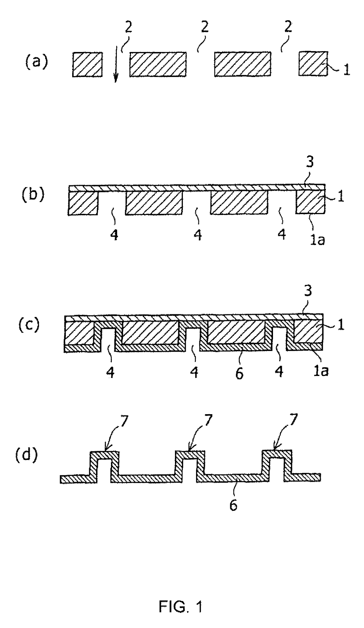
[0053]FIG. 1 is a schematic sectional view showing an embodiment of the process for forming a bump structure in a sequence of steps. A mandrel is defined by a bump-forming die body 1 and a bump-forming die lid joined thereto. Referring to FIG. 1(a), a bump-forming die body 1 is prepared. According to this embodiment, the bump-forming die body 1 is, for example, a rolled copper foil having a thickness of 200 μm. A plurality of through holes 2 are formed in the bump-forming die body. The through holes 2 may be formed in the thickness direction of the rolled copper foil using an NC drill. In this embodiment, the walls of the through holes 2 can be perpendicular to one of the top surface and bottom surface of the bump-forming die body 1. The walls of the through holes 2 can be parallel to each other. This is in contrast to other embodiments, for example, wherein the opening ...


PUM


Abstract

A method for forming a bump structure and a bump structure for conductive interconnection with another element having at least one of microelectronic devices or wiring thereon, used as an electric connection in an electronic circuit, includes the steps of forming a mandrel by steps including forming at least one opening extending through a bump-forming die body in the thickness direction thereof and positioning a bump-forming die lid on a surface of the bump-forming die body so as to cover one end of the opening and to thereby define a bump-forming recess. The bump-forming die body may be comprised of a metal sheet. A metal layer is formed at least on an inner surface of the bump-forming die lid exposed within the bump-forming recess. The mandrel is removed so as to expose the metal layer and form a bump structure.

Description

CROSS-REFERENCE TO RELATED APPLICATIONS[0001]The present application claims the benefit of Japanese Application Ser. No. 2007-295299, filed Nov. 14, 2007, entitled A PROCESS FOR FORMING A BUMP STRUCTURE AND A BUMP STRUCTURE, the disclosure of which is hereby incorporated herein by reference.BACKGROUND OF THE INVENTION[0002]The present invention relates to a process for forming a bump structure in an electronic circuit implementation and the bump structure and, more particularly, relates to a process for forming a bump structure for a circuit implementation in an electronic device such as IC for use in an electronic apparatus, and relates to the bump structure. Further, the present invention relates to a bump-structure forming member for forming the bump-structure, a process for manufacturing thereof, a circuit board having bumps formed thereon and a process for manufacturing thereof.[0003]Conventionally, as a method for connecting an IC chip or the like having a plurality of connect...

Claims


Application Information

Patent Timeline
Patent Type & Authority Patents(United States)
IPC IPC(8): H01L21/44H01L23/043
CPCH01L21/4853H05K3/4007H01L21/4846H01L2224/16225H01L24/81H01L2224/16227H01L2224/81192H01L2224/81399H01L2924/14H01L2924/15311H01L2924/15321H05K3/20H05K2201/0367H05K2203/0113H01L2924/01019H01L2224/81444H01L24/16H01L2924/00014
Inventor ENDO, KIMITAKA
Owner INVENSAS CORP
Why Eureka
Try Eureka