Substrate device having a tuned work function and methods of forming thereof

a substrate device and work function technology, applied in the direction of semiconductor devices, basic electric elements, electrical equipment, etc., can solve the problems of high threshold voltage, poor transistor drive performance, and depletion effect of polysilicon gate electrodes

Active Publication Date: 2012-03-06
APPLIED MATERIALS INC
View PDF5 Cites 7 Cited by
  • Summary
  • Abstract
  • Description
  • Claims
  • Application Information

AI Technical Summary

Problems solved by technology

Unfortunately, polysilicon gate electrodes suffer from a depletion effect.
The depletion effect occurs when the portion of the gate electrode nearest an underlying oxide layer is depleted of dopants, causing the gate electrode layer to behave like an insulating layer, leading to device degradation and eventual malfunction.
For high performance CMOS applications where high-k layers are applied, the polysilicon gate interacts with the high-k film, resulting high threshold voltage and poor transistor drive performance.
However, conventional materials used in metal gate electrodes typically have a limited work function tuning range, making the selection of material limited for each individual need.

Method used


Image

  • Substrate device having a tuned work function and methods of forming thereof
  • Substrate device having a tuned work function and methods of forming thereof
  • Substrate device having a tuned work function and methods of forming thereof

Examples


Embodiment Construction

[0035]Embodiments of the present invention generally relate to semiconductor devices and methods for processing substrates. The inventive methods include methods for forming a device having a tunable work function. The inventive methods may advantageously provide a gate electrode that is not susceptible to dopant depletion and may provide a wide tunable work function range, thereby reducing device degradation and increasing reliability.

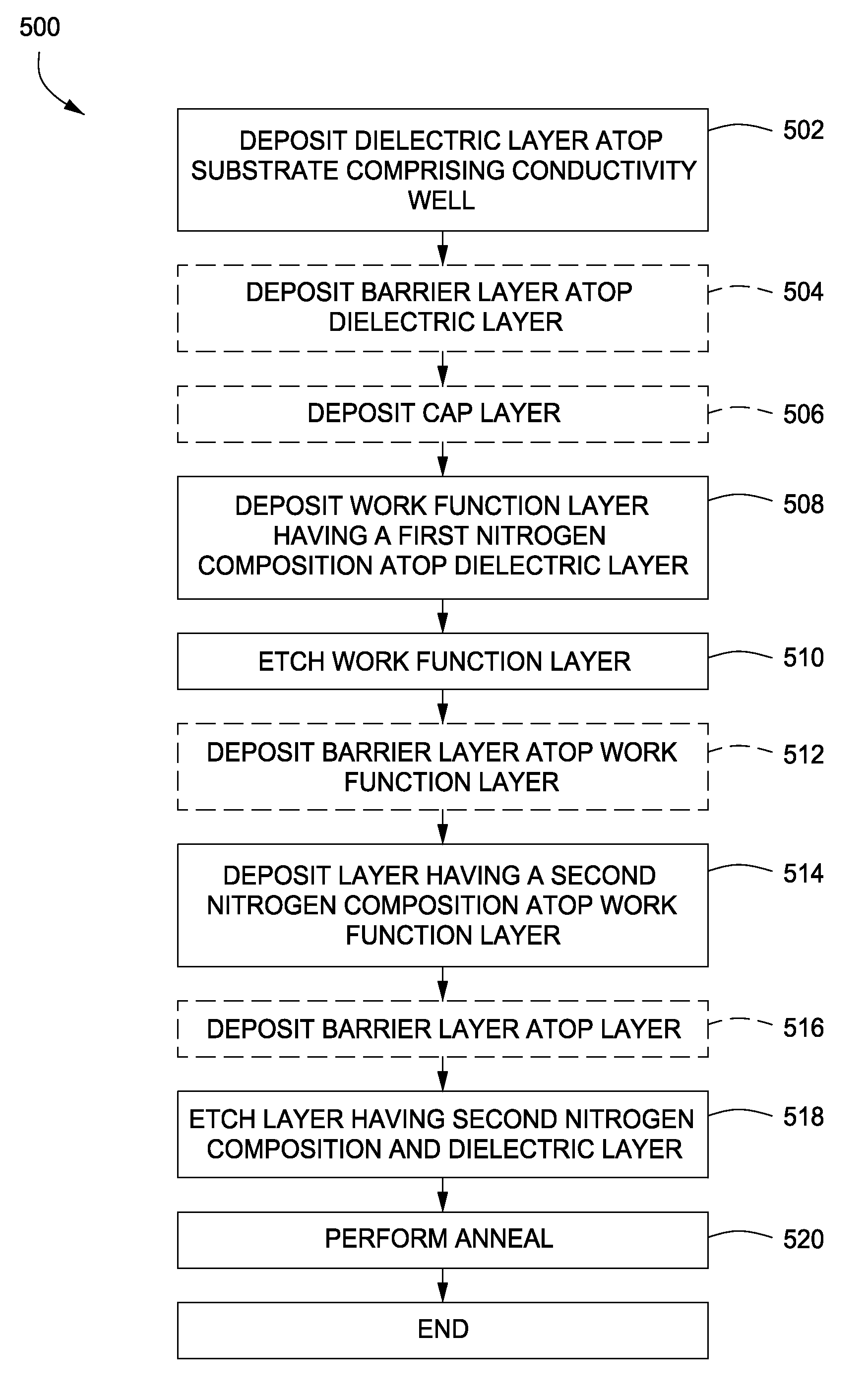
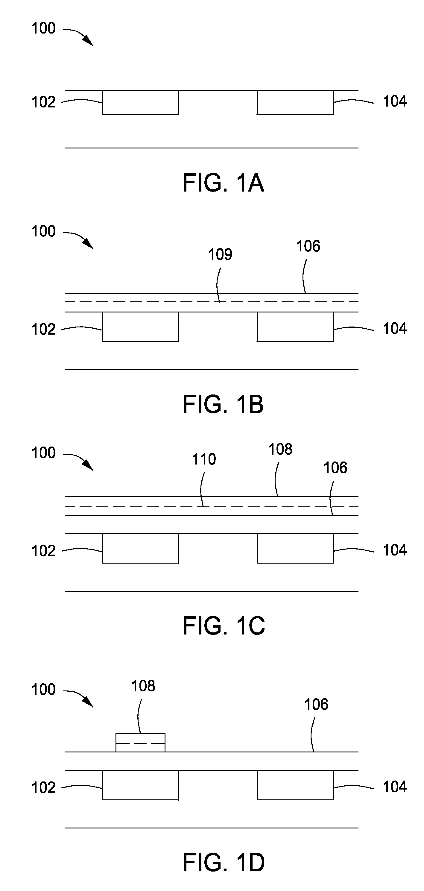
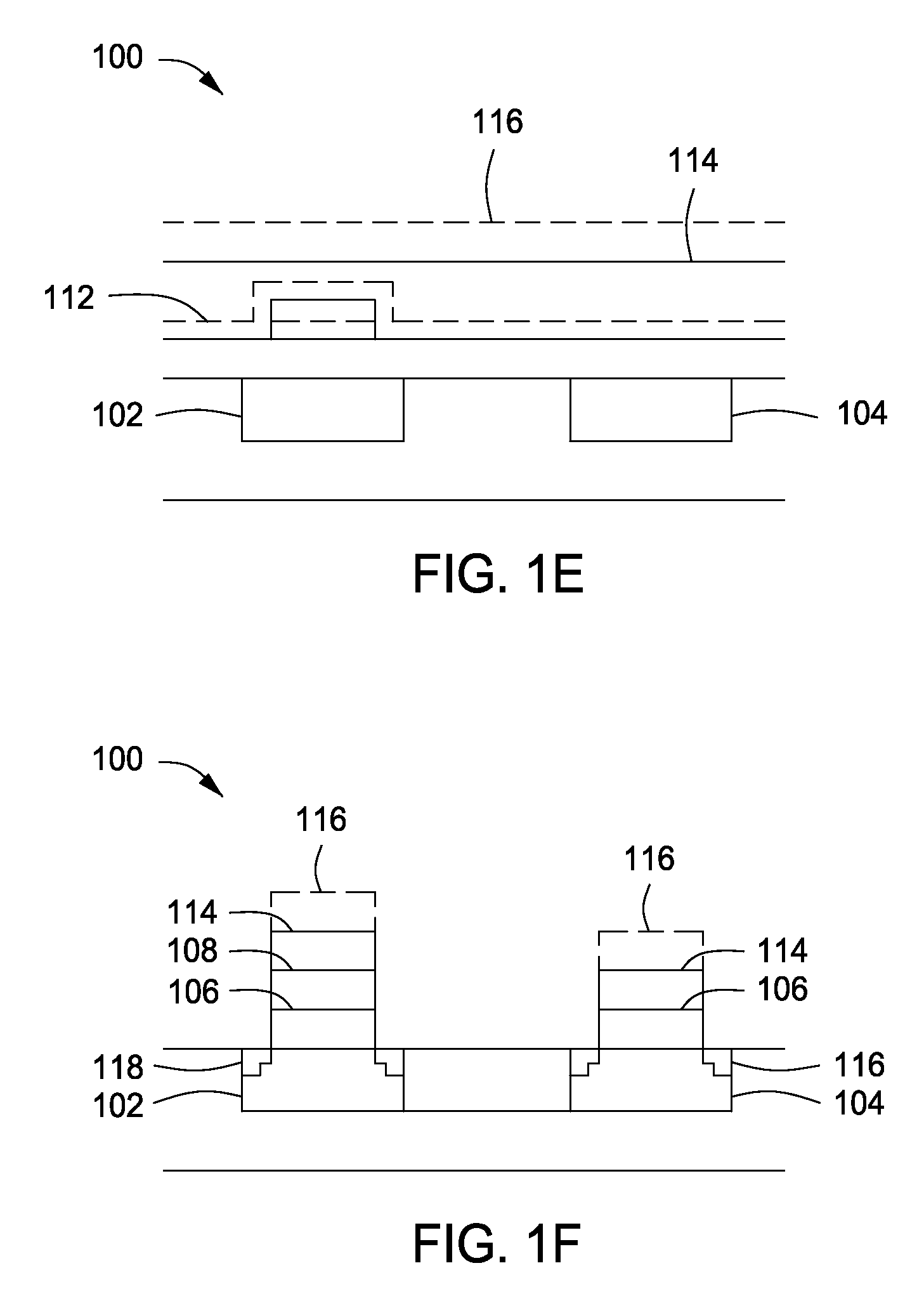
[0036]FIG. 5 depicts a method for processing semiconductor substrates in accordance with some embodiments of the present invention. FIGS. 1A-F depict illustrative cross-sectional views of a substrate during different stages of the method of FIG. 5 with respect to forming a semiconductor device atop a p-type conductivity well, in accordance with some embodiments of the present invention. FIGS. 2A-D depict illustrative cross-sectional views of a substrate during different stages of the method of claim 5 with respect to forming a semiconductor device ato...


PUM

PropertyMeasurementUnit
temperatureaaaaaaaaaa
dielectric constantaaaaaaaaaa
thicknessaaaaaaaaaa

Abstract

Substrate devices having tuned work functions and methods of forming thereof are provided. In some embodiments, forming devices on substrates may include depositing a dielectric layer atop a substrate having a conductivity well; depositing a work function layer comprising titanium aluminum or titanium aluminum nitride having a first nitrogen composition atop the dielectric layer; etching the work function layer to selectively remove at least a portion of the work function layer from atop the dielectric layer; depositing a layer comprising titanium aluminum or titanium aluminum nitride having a second nitrogen composition atop the work function layer and the substrate, wherein at least one of the work function layer or the layer comprises nitrogen; etching the layer and the dielectric layer to selectively remove a portion of the layer and the dielectric layer from atop the substrate; and annealing the substrate at a temperature less than about 1500 degrees Celsius.

Description

BACKGROUND[0001]1. Field[0002]Embodiments of the present invention generally relate to the field of semiconductor manufacturing processes and devices.[0003]2. Description of the Related Art[0004]Integrated circuits may include more than one million micro-electronic field effect transistors or devices (e.g., complementary metal-oxide-semiconductor (CMOS) field effect transistors) that are formed on a substrate and cooperate to perform various functions within the circuit. A CMOS transistor comprises a gate structure disposed over a channel region formed between source and drain regions of the transistor. The gate structure generally comprises a gate electrode and a gate dielectric. The gate electrode is disposed over the gate dielectric and, in operation, is used to control a flow of charge carriers (i.e., electric current) in the channel region beneath the gate dielectric.[0005]In conventional device formation, polysilicon layers are used as gate electrodes. However, the polysilicon...

Claims


Application Information

Patent Timeline
Patent Type & Authority Patents(United States)
IPC IPC(8): H01L21/311
CPCH01L21/28088H01L21/823842H01L21/823857H01L29/4966H01L29/517
Inventor WANG, RONGJUNTANG, XIANMINYANG, DENGLIANGLIU, ZHENDONGGANDIKOTA, SRINIVAS
Owner APPLIED MATERIALS INC
Why Eureka
Try Eureka